background image

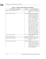
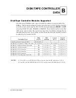
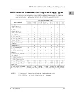
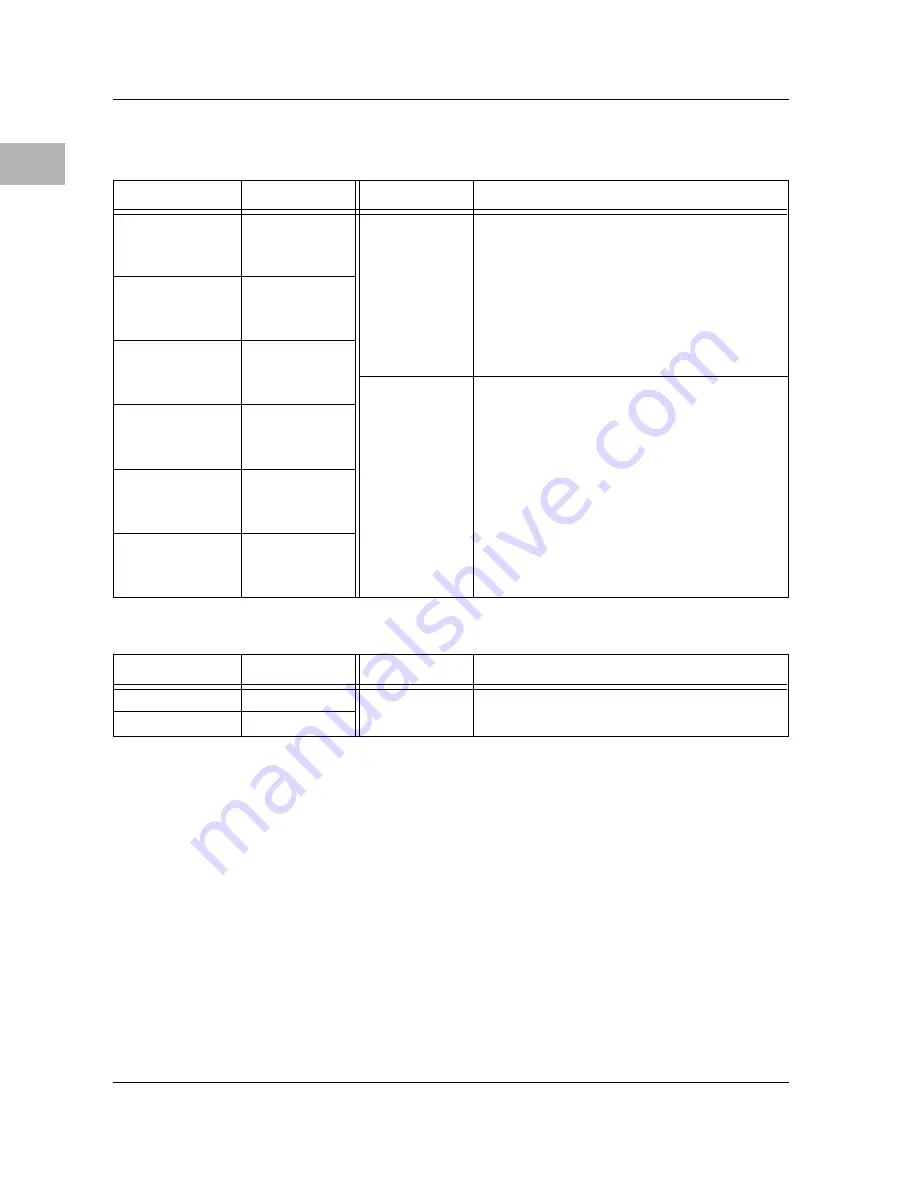
Disk/Tape Controller Data

B-4

MVME166 Single Board Computer Installation Guide

B

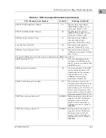
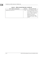
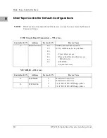
MVME328 -- 14 Devices

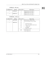
MVME350 -- 1 Device


Controller LUN

Address

Device LUN

Device Type

6

$FFFF9000

00
08
10
18
20
28
30

SCSI Common Command Set
(CCS), which may be any of these:

- Removable flexible direct access

(TEAC style)

- CD-ROM
- Sequential access

7

$FFFF9800

16

$FFFF4800

40
48
50
58
60
68
70

Same as above, but these
will only be available if
the daughter card for the
second SCSI channel is present.

17

$FFFF5800

18

$FFFF7000

19

$FFFF7800

Controller LUN

Address

Device LUN

Device Type

4

$FFFF5000

0

QIC-02 streaming tape drive

5

$FFFF5100

Summary of Contents for MVME166

Page 1: ...MVME166 Single Board Computer Installation Guide MVME166IG D2 ...

Page 2: ...rior written permission of Motorola Inc It is possible that this publication may contain reference to or information about Motorola products machines and programs programming or services that are not announced in your country Such references or information must not be construed to mean that Motorola intends to announce such Motorola products programming or services in your country Restricted Right...

Page 3: ...ded for anyone who wants to provide OEM systems supply additional capability to an existing compatible system or work in a lab environment for experimental purposes A basic knowledge of computers and digital logic is assumed After using this manual you may wish to become familiar with the publications listed in the Related Documentation section in Chapter 1 of this manual This installation guide i...

Page 4: ... to Subpart J of Part 15 of FCC rules which are designed to provide reasonable protection against such interference when operated in a commercial environment Operation of this equipment in a residential area is likely to cause interference in which case the user at the user s own expense will be required to take whatever measures necessary to correct the interference Motorola and the Motorola symb...

Page 5: ...ct electrical outlet or used with a three contact to two contact adapter with the grounding wire green firmly connected to an electrical ground safety ground at the power outlet The power jack and mating plug of the power cable meet International Electrotechnical Commission IEC safety standards Do Not Operate in an Explosive Atmosphere Do not operate the equipment in the presence of flammable gase...

Page 6: ...substitute parts or perform any unauthorized modification of the equipment Contact your local Motorola representative for service and repair to ensure that safety features are maintained Dangerous Procedure Warnings Warnings such as the example below precede potentially dangerous procedures throughout this manual Instructions contained in the warnings must be followed You should also employ all ot...

Page 7: ...AM 1 11 Onboard DRAM 1 12 Battery Backed Up RAM and Clock 1 13 VMEbus Interface 1 13 VME Subsystem Bus VSB Interface 1 13 I O Interfaces 1 13 Serial Port Interface 1 13 MC68230 Parallel Interface Timer 1 14 Parallel Port Interface 1 15 Ethernet Interface 1 15 SCSI Interface 1 16 SCSI Termination 1 16 Local Resources 1 16 Programmable Tick Timers 1 17 Watchdog Timer 1 17 Software Programmable Hardw...

Page 8: ...structions 2 6 MVME166 Module Installation 2 6 System Considerations 2 8 CHAPTER 3 DEBUGGER GENERAL INFORMATION Overview of M68000 Firmware 3 1 Description of 166Bug 3 1 166Bug Implementation 3 3 Installation and Startup 3 3 BOOTBUG 3 7 166BBug Implementation 3 7 Execute User Program 3 8 Setup System Parameters 3 8 Autoboot 3 9 ROMboot 3 10 Network Boot 3 10 Restarting the System 3 11 Reset 3 11 A...

Page 9: ...col Module 3 20 Network Boot Control Module 3 20 Network I O Error Codes 3 20 Multiprocessor Support 3 21 Multiprocessor Control Register MPCR Method 3 21 GCSR Method 3 23 Diagnostic Facilities 3 23 CHAPTER 4 USING THE 166Bug DEBUGGER Entering Debugger Command Lines 4 1 Syntactic Variables 4 2 Expression as a Parameter 4 3 Address as a Parameter 4 4 Address Formats 4 4 Offset Registers 4 6 Port Nu...

Page 10: ...ug Debugger Command Set 4 20 APPENDIX A CONFIGURE AND ENVIRONMENT COMMANDS Configure Board Information Block A 1 Set Environment to Bug Operating System A 2 APPENDIX B DISK TAPE CONTROLLER DATA Disk Tape Controller Modules Supported B 1 Disk Tape Controller Default Configurations B 2 IOT Command Parameters for Supported Floppy Types B 5 APPENDIX C NETWORK CONTROLLER DATA Network Controller Modules...

Page 11: ...xi List of Figures FIGURES Figure 1 1 MVME166 Block Diagram 1 8 Figure 2 1 MVME166 Switches Headers Connectors Fuses and LEDs 2 3 ...

Page 12: ...xii ...

Page 13: ...tions 1 6 Table 1 2 Local Bus Memory Map 1 19 Table 1 3 Local I O Devices Memory Map 1 20 Table 4 1 Debugger Address Parameter Formats 4 5 Table 4 2 Exception Vectors Used by 166Bug 4 11 Table 4 3 Debugger Commands 4 20 Table A 1 ENV Command Parameters A 3 ...

Page 14: ...xiv ...

Page 15: ...r serial ports with TTL interface four tick timers watchdog timer SCSI bus interface with DMA Centronics printer port A16 A24 A32 D8 D16 D32 D64 VMEbus master slave interface VMEbus system controller and a VSB interface The I O connection for the MVME166 is provided by two high density shielded front panel I O connectors The SCSI bus is connected through a 68 pin connector The printer four serial ...

Page 16: ...ected DRAM mezzanine board Related Documentation The MVME166 does not ship with all of the documentation that is available for the product The MVME166 instead ships with a start up installation guide the document you are presently reading that includes all the information necessary to begin working with these products installation instructions jumper configuration information memory maps debugger ...

Page 17: ...nual but has a suffix such as D2A1 the first supplement to the second edition of the manual These manuals may also be ordered in documentation sets as follows 68 MVME166SET for use with the MVME166 MVME166 D MVME167BUG D 68KBUG D SBCSCSI D MVME187PG D SIMVME166 D Document Title Motorola Publication Number Single Board Computers SCSI Software User s Manual SBCSCSI MVME166 MVME167 MVME187 Single Boa...

Page 18: ...cs Engineers Inc 345 East 47th Street New York NY 10017 VSB Specification This is also Parallel Sub system Bus of the IEC 821 VMEbus IEC 822 VSB Bureau Central de la Commission Electrotechnique Internationale 3 rue de Varembé Geneva Switzerland ANSI Small Computer System Interface 2 SCSI 2 Draft Document X3 131 198X Revision 10c Global Engineering Documents P O Box 19539 Irvine CA 92714 CL CD2400 ...

Page 19: ...interface with DMA Four serial ports with TTL buffers Centronics printer port Ethernet transceiver interface with DMA VMEbus interface VMEbus system controller functions VMEbus to local bus interface A24 A32 D8 D16 D32 D8 D16 D32 D64BLT BLT Block Transfer Local bus to VMEbus interface A16 A24 A32 D8 D16 D32 VMEbus interrupter VMEbus interrupt handler Global CSR for interprocessor communications DM...

Page 20: ...6 Specifications Characteristics Specifications Power requirements excluding external LAN transceiver at 33 MHz with 32 MB ECC memory 5 Vdc 5 5 0 A typical 6 5 A max includes transition modules 12 Vdc 5 100 mA max 1 0 A max with offboard LAN transceiver 12 Vdc 5 100 mA max Operating temperature 0 to 55 C at point of entry of forced air approximately 490 LFM Storage temperature 40 to 85 C Relative ...

Page 21: ...t For the MVME166 and other CISC modules this is called a word A four byte is 32 bits numbered 0 through 31 with bit 0 being the least significant For the MVME166 and other CISC modules this is called a longword The terms control bit and status bit are used extensively in this document The term control bit is used to describe a bit in a register that can be set and cleared under software control T...

Page 22: ...1 Block Diagram Figure 1 1 is a general block diagram of the MVME166 Figure 1 1 MVME166 Block Diagram PRINTER PORT CD2401 SCC SERIAL IO 128KB STATIC RAM 53C710 SCSI DRAM FLASH MK48T08 BBRAM CLOCK VSBchip2 MC68040 82596CA LAN ETHERNET PCCchip2 VSB VMEbus VMEchip2 bd078 9304 DOWNLOAD EPROM ...

Page 23: ...us TIP signal line is low This indicates one of the local bus masters is executing a local bus cycle The green SCON LED part of DS2 lights when the VMEchip2 in the MVME166 is the VMEbus system controller The green LAN LED part of DS3 lights when the LAN chip is local bus master The MVME166 supplies 5V 12V and 12V power to the transition board through fuses There is one fuse for each voltage The gr...

Page 24: ...ts replace the four EPROM sockets used on the MVME167 187 The Flash parts are programmable on the MVME166 board and the programming code is provided in the download EPROM The Flash devices provide 1 MB of ROM at address FF800000 FF8FFFFF The download EPROM provides 128 KB of ROM at FFF80000 FFF9FFFF The download EPROM is mapped to local bus address 0 following a local bus reset This allows the MC6...

Page 25: ... the second memory cycle is blocked This allows software to provide an early warning to avoid data loss Because the DS1210S may block the second access the software should do at least two accesses before relying on the data The MVME166 provides jumpers that allow either power source of the DS1210S to be connected to the VMEbus 5 V STDBY pin or one cell of the onboard battery For example the primar...

Page 26: ...nd ignite possibly resulting in injury and or fire When dealing with lithium batteries carefully follow the precautions listed below in order to prevent accidents Do not short circuit Do not disassemble deform or apply excessive pressure Do not heat or incinerate Do not apply solder directly Do not use different models or new and old batteries together Do not charge Always check proper polarity To...

Page 27: ...ap year and 30 day months are automatically made No interrupts are generated by the clock The MK48T08 is an 8 bit device however the interface provided by the PCCchip2 supports 8 16 and 32 bit accesses to the MK48T08 Refer to the MK48T08 data sheet for detailed programming information VMEbus Interface The local bus to VMEbus interface the VMEbus to local bus interface and the local VMEbus DMA cont...

Page 28: ...r detailed programming information The CD2401 supports DMA operations to local memory Because the CD2401 does not support a retry operation necessary to break VMEbus or VSB dual port lockup conditions the CD2401 DMA controllers should not be programmed to access the VMEbus or VSB The hardware does not restrict the CD2401 to onboard DRAM MC68230 Parallel Interface Timer The MVME166 provides an MC68...

Page 29: ...rface The PCCchip2 provides an 8 bit bidirectional parallel port All eight bits of the port must be either inputs or outputs no individual selection In addition to the 8 bits of data there are two control pins and five status pins Each of the status pins can generate an interrupt to the MPU in any of the following programmable conditions high level low level high to low transition or low to high t...

Page 30: ...rd connector is located on the MVME712X transition module Support functions for the 82596CA are provided by the PCCchip2 Refer to the 82596CA user s guide for detailed programming information SCSI Interface The MVME166 provides for mass storage subsystems through the industry standard SCSI bus These subsystems may include hard and floppy disk drives streaming tape drives and other mass storage dev...

Page 31: ...ror Acknowledge TEA signal is sent to the local bus master The timeout value is selectable by software for 8 µsec 64 µsec 256 µsec or infinite The local bus timer does not operate during VMEbus or VSB bound cycles VMEbus bound cycles are timed by the VMEbus access timer and the VMEbus global timer VSB bound cycles are timed by the VSB access timer the VSB transfer timer and if its serial arbiter i...

Page 32: ...nd to the normal access and interrupt acknowledge codes Normal Address Range The memory map of devices that respond to the normal address range is shown in the following tables The normal address range is defined by the Transfer Type TT signals on the local bus On the MVME166 Transfer Types 0 1 and 2 define the normal address range Table 1 2 is the entire map from 00000000 to FFFFFFFF Many areas o...

Page 33: ...e VMEchip2 The local to VSB decoders are programmed in the VSBchip2 3 Size is approximate 4 Cache inhibit depends on devices in area mapped 5 This area is not decoded If these locations are accessed and the local bus timer is enabled the cycle times out and is terminated by a TEA signal Table 1 2 Local Bus Memory Map Address Range Devices Accessed Port Size Size Software Cache Inhibit Notes 000000...

Page 34: ...FF41FFF VSBchip2 D32 D8 4KB 1 10 FFF42000 FFF42FFF PCCchip2 D32 D8 4KB 1 FFF43000 FFF430FF MCECC 1 D8 256B 1 FFF43100 FFF431FF MCECC 2 D8 256B 1 FFF43200 FFF43FFF MCECCs repeated 3 5KB 1 7 FFF44000 FFF44FFF reserved 4KB 5 FFF45000 FFF451FF CD2401 Serial Comm Cont D16 D8 512B 1 9 FFF45200 FFF45DFF reserved 3KB 7 9 FFF45E00 FFF45FFF MC68230 512B 1 9 FFF46000 FFF46FFF 82596CA LAN D32 4KB 1 8 FFF47000...

Page 35: ...e with a TEA signal Writes to the GCSR may be 8 16 or 32 bits Reads to the LCSR and GCSR may be 8 16 or 32 bits 5 This area does not return an acknowledge signal If the local bus timer is enabled the access times out and is terminated by a TEA signal 6 This area does return an acknowledge signal 7 Size is approximate 8 Port commands to the 82596CA must be written as two 16 bit writes upper word fi...

Page 36: ...program the starting and ending address and the modifiers the MVME166 responds to VMEbus Short I O Memory Map The VMEchip2 includes a user programmable map decoder for the GCSR The GCSR map decoder allows you to program the starting address of the GCSR in the VMEbus short I O space VSB Memory Map This section describes the mapping of local resources as viewed by VSB masters The VSBchip2 on the MVM...

Page 37: ...ify that all items are present Save packing material for storing and reshipping of equipment Caution Avoid touching areas of integrated circuitry static discharge can damage circuits Hardware Preparation To select the desired configuration and ensure proper operation of the MVME166 certain option modifications may be necessary before installation The MVME166 provides software control for most of t...

Page 38: ...tory installed Debug Monitor MVME166Bug 166Bug with these factory jumper settings Settings can be changed for the following headers SCSI terminator selection J2 General purpose readable register J3 System controller selection J6 SRAM backup power source selection J7 SCSI Terminator Enable Header J2 The MVME166 provides terminators for the SCSI bus The SCSI terminators are enabled disabled by jumpe...

Page 39: ...LEDs S1 S2 P1 A1 B1 C1 A32 B32 C32 1381 9404 MVME 166 LGA PRIMARY SIDE P2 A32 B32 C32 A1 B1 C1 DS4 DS3 DS2 DS1 1 2 J8 SCSI STAT FAIL RUN SCON LAN RPWR SCSI VME ABORT RESET 34 33 68 67 2 1 36 35 DS5 J9 49 50 99 100 1 2 51 22 F1 F3 F4 J3 J6 2 16 1 1 2 6 F2 I O 2 15 1 5 J7 J2 MEZZANINE BOARD TPWR VSB ...

Page 40: ... zero when the jumper is on System Controller Header J6 The MVME166 can operate as VMEbus system controller The system controller function is enabled disabled by jumpers on header J6 When the MVME166 is functioning as system controller the SCON LED is turned on The VMEchip2 can be configured as a system controller as follows 15 GPIO0 GPIO1 GPIO2 GPIO6 GPIO3 GPIO4 GPIO5 1 2 16 GPIO7 All Zeros 7 8 J...

Page 41: ...y is removed jumpers must be installed on J7 between pins 1 to 3 and pins 2 to 4 as shown in the Factory Configuration drawing above J7 1 5 2 6 Primary Source OnboardBattery Secondary Source Onboard Battery J7 1 5 2 6 Primary Source VMEbus 5V STBY Secondary Source VMEbus 5V STBY Factory Configuration J7 1 5 2 6 Primary Source VMEbus 5V STBY Secondary Source Onboard Battery J7 1 5 2 6 Primary Sourc...

Page 42: ...disconnect power cable from ac power source Caution Inserting or removing modules while power is applied could result in damage to module components WARNING DANGEROUS VOLTAGES CAPABLE OF CAUSING DEATH ARE PRESENT IN THIS EQUIPMENT USE EXTREME CAUTION WHEN HANDLING TESTING AND ADJUSTING b Remove chassis cover as instructed in the equipment user s manual c Remove the filler panel s from the appropri...

Page 43: ...t Be sure the module is seated properly in the P1 and P2 connectors on the backplane Do not damage or bend connector pins Fasten the module in the chassis with the screws provided making good contact with the transverse mounting rails to minimize RFI emissions e On the chassis backplane remove the IACK and BG jumpers from the header for the card slot occupied by the MVME166 f Connect the transitio...

Page 44: ...dditional memory and I O over a local bus removing traffic from the global VMEbus and improving the total throughput of the system The VSB interface occupies 64 I O pins on connector P2 and utilizes the multiplexing of address and data in order to achieve full 32 bit functionality along with appropriate control signals within the 64 pin allotment The MVME166 contains shared onboard DRAM whose base...

Page 45: ...reset connector These voltage sources are used by the transition modules to power the serial port drivers and any LAN transceivers connected to the transition module The RPWR LED DS3 on the MVME166 front panel lights when all three voltages are available The MVME166 provides 5 Vdc to the SCSI bus TERMPWR signal through fuse F2 located near the front panel SCSI bus connector The TPWR LED DS5 on the...

Page 46: ...Hardware Preparation and Installation 2 10 MVME166 Single Board Computer Installation Guide 2 ...

Page 47: ...he MVME166 CISC based microcomputers Facilities are available for loading and executing user programs under complete operator control for system evaluation 166Bug includes commands for display and modification of memory breakpoint and tracing capabilities a powerful assembler disassembler useful for patching programs and a self test at power up feature which verifies the integrity of the system Va...

Page 48: ...mmand or may examine the commands in the particular directory that you are currently in by using the Help HE command Because 166Bug is command driven it performs its various operations in response to user commands entered at the keyboard When you enter a command 166Bug executes the command and the prompt reappears However if you enter a command that causes execution of user target code e g GO then...

Page 49: ...consumes the first half 512KB of this memory leaving the second half available for user applications A command is provided both in the regular Bug product and the BootBug product to allow erasing and reprogramming this Flash memory WARNING Reprogramming any portion of Flash memory will erase everything currently contained in Flash including the 166Bug product You must copy the 166Bug from Flash to...

Page 50: ...ult condition is with all eight jumpers installed between pins 1 2 3 4 5 6 7 8 9 10 11 12 13 14 and 15 16 The MVME166 may be configured with these readable jumpers These jumpers can be read as a register at FFF40088 in the VMEchip2 LCSR The bit values are read as a one when the jumper is off and as a zero when the jumper is on This jumper block header J3 contains eight bits Refer to the MVME166 MV...

Page 51: ... is a one high it instructs the debugger to use the default setup operation parameters in ROM versus the user setup operation parameters in NVRAM This is the same as depressing the RESET and ABORT switches at the same time This feature can be used in the event the user setup is corrupted or does not meet a sanity check Refer to the ENV command Appendix A for the ROM defaults Bit 2 GPI2 5 6 Reserve...

Page 52: ...the terminal must do some form of handshaking If the terminal being used does not do hardware handshaking via the CTS line then it must do XON XOFF handshaking If you get garbled messages and missing characters then you should check the terminal to make sure XON XOFF handshaking is enabled 5 If you want to connect devices such as a host computer system and or a serial printer to the other EIA 232 ...

Page 53: ... the VMEbus serial port SCSI bus or the network and reprogramming of the Flash memory The following table lists the the new commands available in the 166BBug product Detailed descriptions of additional subset commands can be found in the Debugging Package for Motorola 68K CISC CPUs User s Manual There is a jumper on the MVME166 board that controls the operation of the BootBug If the jumper at J3 p...

Page 54: ...input The SETUP command VME parameters do not stay through a reset These parameters are not saved to NVRAM The remaining parameters MPU Clock Speed Ethernet Address Local SCSI Identifier are saved to NVRAM but are not checksummed 166 Bug setup MPU Clock Speed 3300 Ethernet Address 000000000000 Local SCSI Identifier 07 VME Slave Enable Y N N VME Slave Starting Address 00000000 VME Slave Ending Addr...

Page 55: ...u an opportunity to abort the Autoboot process if you wish Then the actual I O is begun the program pointed to within the volume ID of the media specified is loaded into RAM and control passed to it If however during this time you want to gain control without Autoboot you can press the BREAK key or the software ABORT or RESET switches Autoboot is controlled by parameters contained in the ENV comma...

Page 56: ...ction For a user s ROMboot module to gain control through the ROMboot linkage four requirements must be met a Power must have just been applied but the ENV command can change this to also respond to any reset b Your routine must be located within the MVME166 ROM memory map but the ENV command can change this to any other portion of the onboard memory or even offboard VMEbus memory c The ASCII stri...

Page 57: ... of the Boot delay Refer to the ENV command in Appendix A for more details Restarting the System You can initialize the system to a known state in three different ways reset abort and break Each has characteristics which make it more appropriate than the others in certain situations The debugger has a special feature upon a reset condition This feature is activated by depressing the RESET and ABOR...

Page 58: ...unction Pressing and releasing the ABORT switch generates a local board condition which may interrupt the processor if enabled The target registers reflecting the machine state at the time the ABORT switch was pressed are displayed on the screen Any breakpoints installed in your code are removed and the breakpoint table remains intact Control is returned to the debugger Break A Break is generated ...

Page 59: ... a warning message is displayed The calculated clock speed is also checked against known clock speeds and tolerances Memory Requirements The program portion of 166Bug is approximately 512KB of code consisting of download debugger anddiagnostic packages and containedentirely in Flash The Flash memory on the MVME166 is mapped starting at location FF800000 166Bug requires a minimum of 64KB of contigu...

Page 60: ...and then a carriage return and line feed is issued along with another prompt H backspace The cursor is moved back one position The character at the new cursor position is erased If the hardcopy option is selected a character is typed along with the deleted character DEL delete or rubout Performs the same function as H D redisplay The entire command line as entered so far is redisplayed on the foll...

Page 61: ...but may be altered as described in the section on default parameters later in this chapter Appendix B contains a list of the controllers presently supported as well as a list of the default configurations for each controller Blocks Versus Sectors The logical block defines the unit of information for disk devices A disk is viewed by 166Bug as a storage area divided into logical blocks By default th...

Page 62: ... Detailed instructions for their use are found in the Debugging Package for Motorola 68K CISC CPUs User s Manual When a command is issued to a particular controller LUN and device LUN these LUNs are remembered by 166Bug so that the next disk command defaults to use the same controller and device IOI Input Output Inquiry This command is used to probe the system for all possible CLUN DLUN combinatio...

Page 63: ...ly by 166Bug TRAP 15 system calls The command level disk operations provide a convenient way of using these system calls without writing and executing a program The following system calls are provided to allow user programs to do disk I O Refer to the Debugging Package for Motorola 68K CISC CPUs User s Manual for information on using these and other system calls DSKRD Disk read System call to read...

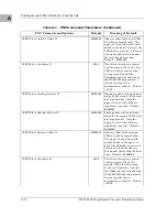
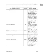
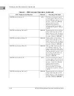
Page 64: ...red for the disk drive controller it is sent to Refer to documentation on the particular controller module for the format of its packets and for using the IOC command Default 166Bug Controller and Device Parameters 166Bug initializes the parameter tables for a default configuration of controllers and devices refer to Appendix B If the system needs to be configured differently than this default con...

Page 65: ...boot function are described in the following paragraphs Intel 82596 LAN Coprocessor Ethernet Driver This driver manages surrounds the Intel 82596 LAN Coprocessor Management is in the scope of the reception of packets the transmission of packets receive buffer flushing and interface initialization This module ensures that the packaging and unpackaging of Ethernet packets is done correctly in the Bo...

Page 66: ... a server host and the name of a file to be loaded into memory and executed TFTP Protocol Module The Trivial File Transfer Protocol TFTP is a simple protocol to transfer files It is implemented on top of the Internet User Datagram Protocol UDP or Datagram so it may be used to move files between machines on different networks implementing UDP The only thing it can do is read and write files from to...

Page 67: ...essors The MPCR contents are organized as follows The status codes stored in the MPCR are of two types Status returned from the monitor Status set by the bus master The status codes that may be returned from the monitor are You can only program Flash memory by the MPCR method Refer to the PFLASH system call in the Debugging Package for Motorola 68K CISC CPUs User s Manual for a description of the ...

Page 68: ...lete Then the prompt is sent If no terminal is connected to the port the MPCR is still polled to see whether an external processor requires control to be passed to the dual port RAM If a terminal does respond the MPCR is polled for the same purpose while the serial port is being polled for user input An ASCII G placed in the MPCR by a remote processor indicates that the Go Direct type of transfer ...

Page 69: ...t value and the board select value programmed in the Local Control and Status Registers LCSR of the MVME166 The execution address is formed by reading the GCSR general purpose registers in the following manner The address appears as Diagnostic Facilities The 166Bug package includes a complete set of hardware diagnostics intended for testing and troubleshooting of the MVME166 These diagnostics are ...

Page 70: ...Debugger General Information 3 24 MVME166 Single Board Computer Installation Guide 3 ...

Page 71: ...tion of user target code for example GO then control may or may not return to the debugger depending on what the user program does For example if a breakpoint has been specified then control returns to the debugger when the breakpoint is encountered during execution of the user program Alternately the user program could return to the debugger by means of the TRAP 15 function RETURN In general a de...

Page 72: ...actic variable and is to be replaced by one of a class of items it represents A vertical bar separating two or more items indicates that a choice is to be made only one of the items separated by this symbol should be selected Square brackets enclose an item that is optional The item may appear zero or one time Braces enclose an optional symbol that may occur zero or more times DEL Delimiter either...

Page 73: ...f up to four characters The string literal must begin and end with the single quote mark The numeric value is interpreted as the concatenation of the ASCII values of the characters This value is right justified as any other numeric value would be Evaluation of an expression is always from left to right unless parentheses are used to group part of the expression There is no operator precedence Sube...

Page 74: ...yntax accepted by 166Bug is similar to the one accepted by the MC68040 one line assembler All control addressing modes are allowed An address offset register mode is also provided Address Formats Table 4 1 summarizes the address formats which are acceptable for address parameters in debugger command lines Expression Result In Hex Notes FF0011 FF0011 45 99 DE 45 99 90 35 67 10 5C 10011110 1001 A7 8...

Page 75: ...ormats accepted d An Xn or d An Xn 120 A1 D2 120 A1 D2 Address register indirect with index and displacement two formats accepted bd An Xn od C A2 A3 100 Memory indirect preindexed bd An Xn od 12 A3 D2 10 Memory indirect postindexed For the memory indirect modes fields can be omitted For example three of many permutations are as follows An od A1 4 bd FC1E bd Xn 8 D2 NOTES N Absolute address any va...

Page 76: ...y 0 that is not the one at which they are loaded so it is harder to correlate addresses in the listing with addresses in the loaded program The offset registers solve this problem by taking into account this difference and forcing the display of addresses in a relative address offset format Offset registers have adjustable ranges and may even have overlapping ranges The range for each offset regis...

Page 77: ...0000000A 12D8 LOOP MOVE B A0 A1 10 0 0000000C 51C8FFFC MOVS DBRA D0 LOOP 11 0 00000010 4CDF0101 MOVEM L A7 D0 A0 12 0 00000014 4E75 RTS 13 14 END TOTAL ERRORS 0 TOTAL WARNINGS 0 The above program was loaded at address 0001327C The disassembled code is shown next 166Bug MD 1327C DI 0001327C 48E78080 MOVEM L D0 A0 A7 00013280 4280 CLR L D0 00013282 1018 MOVE B A0 D0 00013284 5340 SUBQ W 1 D0 0001328...

Page 78: ...ing Package for Motorola 68K CISC CPUs User s Manual Port Numbers Some 166Bug commands give you the option to choose the port to be used to input or output Valid port numbers which may be used for these commands are as follows 1 MVME166 EIA 232 D Debug Terminal Port 0 or 00 PORT 1 on the MVME166 J9 connector Sometimes known as the console port it is used for interactive user input output by defaul...

Page 79: ...tallation and Startup in Chapter 3 The file is downloaded from the host to MVME166 memory by the Load LO command Another way is by reading in the program from disk using one of the disk commands BO BH IOP Once the object code has been loaded into memory you can set breakpoints if desired and run the code or trace through it Yet another way is via the network using one of the network disk commands ...

Page 80: ...les 166Bug allocates space for the system stack then initializes the system stack pointer to the top of this area With the exception of the first 1024 byte vector table area you must be extremely careful not to use the above mentioned memory areas for other purposes You should refer to the Memory Requirements section in Chapter 3 to determine how to dictate the location of the reserved memory area...

Page 81: ...e target stack pointer is left pointing past the bottom of the exception stack frame created that is it reflects the system stack pointer values just before the exception occurred In this way the operation of the debugger facility through an exception is transparent to users Table 4 2 Exception Vectors Used by 166Bug Vector Offset Exception 166Bug Facility 10 Illegal instruction Breakpoints used b...

Page 82: ... 00000000 A4 00000000 A5 00000000 A6 00000000 A7 0000FFFC 00010006 D280 ADD L D0 D1 166Bug Notice that the value of the target stack pointer register A7 has not changed even though a trace exception has taken place Your program may either use the exception vector table provided by 166Bug or it may create a separate exception vector table of its own The two following sections detail these two metho...

Page 83: ...ifications to the vectors contained in it Creating a New Vector Table Your program may create a separate vector table in memory to contain its exception vectors If this is done the program must change the value of the VBR to point at the new vector table In order to use the debugger facilities you can copy the proper vectors from the 166Bug vector table into the corresponding vector locations in y...

Page 84: ...y turn out that your program uses one or more of the exception vectors that are required for debugger operation Debugger facilities may still be used however if your exception handler can determine when to handle the exception itself and when to pass the exception to the debugger When an exception occurs which you want to pass on to the debugger i e ABORT your exception handler must read the vecto...

Page 85: ... 4 A6 Store address of debugger exc handler MOVEM L SP A0 A5 D0 D7 Restore registers UNLK A6 RTS Put addr of exc handler into PC and go 166Bug Generalized Exception Handler The 166Bug has a generalized exception handler which it uses to handle all of the exceptions not listed in Table 4 2 For all these exceptions the target stack pointer is left pointing to the top of the exception stack frame cre...

Page 86: ...8 PC 00010000 SR 2708 TR OFF_S _7_ N VBR 00000000 USP 0000DFFC MSP 0000EFFC ISP 0000FFFC SFC 0 F0 DFC 0 F0 CACR 0 D0 00000001 D1 00000001 D2 00000000 D3 00000000 D4 00000000 D5 00000002 D6 00000000 D7 00000000 A0 00000000 A1 00000000 A2 00000000 A3 00000000 A4 00000000 A5 00000000 A6 00000000 A7 0000FFC0 00010000 203900F0 0000 MOVE L F00000 L D0 166Bug Notice that the target stack pointer is diffe...

Page 87: ...The sign field is the first field and is a binary field 2 The exponent field is the second field and is a hexadecimal field 3 The mantissa field is the last field and is a hexadecimal field 4 The sign field the exponent field and at least the first digit of the mantissa field must be present any unspecified digits in the mantissa field are set to zero 5 Each field must be separated from adjacent f...

Page 88: ...le precision formats have an implied integer bit always 1 Extended Precision Real This format would appear in memory as An extended precision number takes 10 bytes in memory 1 bit sign field 1 binary digit 8 bit biased exponent field 2 hex digits Bias 7F 23 bit fraction field 6 hex digits 1 bit sign field 1 binary digit 11 bit biased exponent field 3 hex digits Bias 3FF 52 bit fraction field 13 he...

Page 89: ...cified data type Entering data in this format requires the following fields An optional sign bit or One decimal digit followed by a decimal point Up to 17 decimal digits at least one must be entered An optional Exponent field that consists of An optional underscore The Exponent field identifier letter E An optional Exponent sign From 1 to 3 decimal digits For more information about the MC68040 flo...

Page 90: ...H DEL Controller LUN DEL Device LUN DEL String BI Block of Memory Initialize BI RANGE B W L BM Block of Memory Move BM RANGE DEL ADDR B W L BO Bootstrap Operating System BO DEL Controller LUN DEL Device LUN DEL String BR Breakpoint Insert BR ADDR COUNT NOBR Breakpoint Delete NOBR ADDR BS Block of Memory Search BS RANGE DEL TEXT B W L or BS RANGE DEL data DEL mask B W L N V BV Block of Memory Verif...

Page 91: ...ce LUN DEL block MD Memory Display MD S ADDR COUNT ADDR B W L S D X P DI MENU Menu MENU MM Memory Modify MM ADDR B W L S D X P A N DI MMD Memory Map Diagnostic MMD RANGE DEL increment B W L MS Memory Set MS ADDR Hexadecimal number string MW Memory Write MW ADDR DATA B W L NAB Automatic Network Boot Operating System NAB NBH Network Boot Operating System and Halt NBH Controller LUN Device LUN Client...

Page 92: ...L ADDR B W L RM Register Modify RM REG S D RS Register Set RS REG DEL EXP DEL ADDR S D SD Switch Directories SD SET Set Time and Date SET mmddyyhhmm or SET n C SYM Symbol Table Attach SYM ADDR NOSYM Symbol Table Detach NOSYM SYMS Symbol Table Display Search SYMS symbol name S T Trace T COUNT TA Terminal Attach TA port TC Trace on Change of Control Flow TC count TIME Display Time and Date TIME C L ...

Page 93: ...he current contents of the board information block 166 Bug cnfg Board PWA Serial Number 000000061050 Board Identifier MVME166 11 Artwork PWA Identifier 01 W3834B01B MPU Clock Speed 3300 Ethernet Address 08003E20A867 Local SCSI Identifier 07 Optional Board 1 Artwork PWA Identifier Optional Board 1 PWA Serial Number Optional Board 2 Artwork PWA Identifier Optional Board 2 PWA Serial Number 166 Bug N...

Page 94: ...ational parameters that are kept in Battery Backed Up RAM BBRAM also known as Non Volatile RAM NVRAM The operational parameters are saved in NVRAM and used whenever power is lost Any time the Bug uses a parameter from NVRAM the NVRAM contents are first tested by checksum to insure the integrity of the NVRAM contents In the instance of BBRAM checksum failure certain default values are assumed as st...

Page 95: ...ter successful completion or entrance into the bug command monitor Local SCSI Bus Reset on Debugger Startup Y N N Local SCSI bus is not reset on debugger startup Local SCSI Bus Negotiations Type A S N A Asynchronous Ignore CFGA Block on a Hard Disk Boot Y N Y Enable the ignorance of the Configuration Area CFGA Block hard disk only Auto Boot Enable Y N N Auto Boot function is disabled Auto Boot at ...

Page 96: ... Direct Starting Address FF800000 First location tested when the Bug searches for a ROMboot Module ROM Boot Direct Ending Address FFBFFFFC Last location tested when the Bug searches for a ROMboot Module Network Auto Boot Enable Y N N Network Auto Boot function is disabled Network Auto Boot at power up only Y N Y Network Auto Boot is attempted at power up reset only Network Auto Boot Controller LUN...

Page 97: ...gers to operate simultaneously Memory Search Ending Address 02000000 Top limit of the Bug s search for a work page If a contiguous block of memory 64KB in size is not found in the range specified by Memory Search Starting Address and Memory Search Ending Address parameters then the bug will place its work page in the onboard static RAM on the MVME166 Default Memory Search Ending Address is the cal...

Page 98: ...mary CPUs will wait for the data at the Memory Search Delay Address to be set to 00 01 or 02 refer to the Memory Requirements section in Chapter 3 for the definition of these values before attempting to locate their work page in the memory of the primary CPU Memory Size Enable Y N Y Memory will be sized for Self Test diagnostics Memory Size Starting Address 00000000 Default Starting Address is 0 M...

Page 99: ...ng address of the local resource that is accessible by the VMEbus Default is the end of calculated memory Slave Address Translation Address 1 00000000 This register will allow the VMEbus address and the local address to be different The value in this register is the base address of local resource that is associated with the starting and ending address selection from the previous questions Default ...

Page 100: ...s decoder Default is 01EF Master Enable 1 Y N Y Yes Setup and enable the Master Address Decoder 1 Master Starting Address 1 02000000 Base address of the VMEbus resource that is accessible from the local bus Default is the end of calculated local memory unless memory is less than 16MB then this register will always be set to 01000000 Master Ending Address 1 EFFFFFFF Ending address of the VMEbus res...

Page 101: ...ble from the local bus If enabled the value is calculated as one less than the calculated size of memory If not enabled the default is 00000000 Master Ending Address 3 00000000 Ending address of the VMEbus resource that is accessible from the local bus If enabled the default is 00FFFFFF otherwise 00000000 Master Control 3 00 Defines the access characteristics for the address space defined with thi...

Page 102: ... address decoder Default is 00 Short I O VMEbus A16 Enable Y N Y Yes Enable the Short I O Address Decoder Short I O VMEbus A16 Control 01 Defines the access characteristics for the address space defined with the Short I O address decoder Default is 01 F Page VMEbus A24 Enable Y N Y Yes Enable the F Page Address Decoder F Page VMEbus A24 Control 02 Defines the access characteristics for the address...

Page 103: ...ith this ENV option VSBC2 Interrupt Vector Base 0E Vector passed back to the VSB master during the Status ID transfer phase of an interrupt acknowledge cycle if the VSBchip2 wins interrupt arbitration Default 0E VSBC2 Local Interrupt Vector Base 00 The value here is part of the interrupt vector supplied on the local bus during an interrupt acknowledge cycle The lower 4 bits are reserved and are re...

Page 104: ...local bus map decoder Only the upper 16 bits of this field are significant or used Default 00000000 VSBC2 Slave Ending Address 2 00000000 Ending address of an address range for the second VSB to local bus map decoder Only the upper 16 bits of this field are significant or used Default 00000000 VSBC2 Slave Address Offset 2 00000000 Address offset for the second VSB to local bus map decoder The uppe...

Page 105: ...r VSB accesses Definition of the register contents can be found in the MVME166 programmer s reference guide Default 1000 VSBC2 Master Starting Address 1 00000000 Beginning address of an address range for the local bus to VSB map decoder 1 Only the upper 16 bits of this field are significant or used Default 00000000 VSBC2 Master Ending Address 1 00000000 Ending address of an address range for the l...

Page 106: ...s of this field are significant or used Default 00000000 VSBC2 Master Address Offset 2 00000000 Address offset for the local bus to VSB map decoder 2 The upper 16 bits of this field will be added to the upper 16 bits of the local bus address received This sum is then the address driven onto the VSB address lines Default 00000000 VSBC2 Master Attributes 2 0030 The bits in this register control vari...

Page 107: ...chip2 register definition in the MVME166 programmer s reference guide for a detailed explanation of each bit Default 0030 VSBC2 Master Starting Address 4 00000000 Beginning address of an address range for the local bus to VSB map decoder 4 Only the upper 16 bits of this field are significant or used Default 00000000 VSBC2 Master Ending Address 4 00000000 Ending address of an address range for the ...

Page 108: ...s in this register control various aspects of how the local bus to VSB map decoder 4 will operate Consult the VSBchip2 register definition in the MVME166 programmer s reference guide for a detailed explanation of each bit Default 0030 Table A 1 ENV Command Parameters Continued ENV Parameter and Options Default Meaning of Default ...

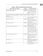
Page 109: ...Second Address and can be called up by Second CLUN Controller Type First CLUN First Address Second CLUN Second Address CISC Single Board Computer SBC 00 NOTE 1 MVME320 Winchester Floppy Controller 11 NOTE 2 FFFFB000 12 NOTE 2 FFFFAC00 MVME323 ESDI Winchester Controller 08 FFFFA000 09 FFFFA200 MVME327A SCSI Controller 02 FFFFA600 03 FFFFA700 MVME328 SCSI Controller 06 FFFF9000 07 FFFF9800 MVME328 S...

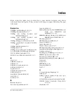
Page 110: ... tested by Motorola Computer Group Controller LUN Address Device LUN Device Type 0 XXXXXXXX 00 10 20 30 40 50 60 SCSI Common Command Set CCS which may be any of these Fixed direct access Removable flexible direct access TEAC style CD ROM Sequential access Controller LUN Address Device LUN Device Type 11 FFFFB000 0 1 2 3 Winchester hard drive Winchester hard drive 5 1 4 DS DD 96 TPI floppy drive 12...

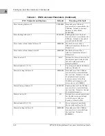
Page 111: ...r hard drive ESDI Winchester hard drive ESDI Winchester hard drive 9 FFFFA200 ESDI Winchester hard drive Controller LUN Address Device LUN Device Type 2 FFFFA600 00 10 20 30 40 50 60 SCSI Common Command Set CCS which may be any of these Fixed direct access Removable flexible direct access TEAC style CD ROM Sequential access 3 FFFFA700 80 81 Local floppy drive Local floppy drive ...

Page 112: ...Common Command Set CCS which may be any of these Removable flexible direct access TEAC style CD ROM Sequential access 7 FFFF9800 16 FFFF4800 40 48 50 58 60 68 70 Same as above but these will only be available if the daughter card for the second SCSI channel is present 17 FFFF5800 18 FFFF7000 19 FFFF7800 Controller LUN Address Device LUN Device Type 4 FFFF5000 0 QIC 02 streaming tape drive 5 FFFF51...

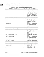
Page 113: ... 50 50 50 50 Precomp Cylinder 50 28 28 50 50 50 50 Reduced Write Current Cylinder 50 28 28 50 50 50 50 Step Rate Code 0 0 0 0 0 0 0 Single Double DATA Density D D D D D D D Single Double TRACK Density D D D D D D D Single Equal_in_all Track Zero Density S E E E E E E Slow Fast Data Rate S S S S F F F Other Characteristics Number of Physical Sectors 0A00 0280 02D0 05A0 0960 0B40 1680 Number of Logi...

Page 114: ...Disk Tape Controller Data B 6 MVME166 Single Board Computer Installation Guide B ...

Page 115: ...ith the debugger commands NBH NBO NIOP NIOC NIOT NPING and NAB and also with the debugger system calls NETRD NETWR NETFOPN NETFRD NETCFIG and NETCTRL Controller Type CLUN DLUN Address Interface Type MVME166 00 00 FFF46000 Ethernet MVME376 02 00 FFFF1200 Ethernet MVME376 03 00 FFFF1400 Ethernet MVME376 04 00 FFFF1600 Ethernet MVME376 05 00 FFFF5400 Ethernet MVME376 06 00 FFFF5600 Ethernet MVME376 0...

Page 116: ...Network Controller Data C 2 MVME166 Single Board Computer Installation Guide C ...

Page 117: ...ss formats 4 4 arguments 4 1 arithmetic operators 4 3 ASCII string 4 2 assembler disassembler 4 9 assertion 1 7 autoboot 3 9 B Backus Naur 4 2 base and top addresses 4 6 base identifier 4 3 Battery Backed Up RAM BBRAM and Clock see MK48T08 and NVRAM 1 13 A 1 BBRAM Battery Backed Up RAM see MK48T08 and NVRAM 1 13 BG bus grant 2 7 BH Bootstrap and Halt 3 17 binary number 1 6 block diagram 1 8 blocks...

Page 118: ...1 device LUN DLUN B 2 C 1 device probe function 3 16 diagnostic facilities 3 23 direct access device B 2 B 4 disk I O error codes 3 19 disk I O support 3 15 disk I O via 166Bug commands 3 16 disk I O via 166Bug system calls 3 17 disk tape controller data B 1 disk tape controller default configura tions B 2 disk tape controller modules supported B 1 DLUN device LUN B 2 C 1 double precision real 4 1...

Page 119: ...on and installation 2 1 headers 3 4 hexadecimal character 1 6 host port 4 8 host system 4 9 I I O interfaces 1 13 IACK interrupt acknowledge 2 7 indicators 1 9 installation 3 3 installation and startup 3 3 installation instructions 2 6 Intel 82596 LAN Coprocessor Ethernet driver 3 19 interrupt acknowledge IACK 2 7 Interrupt Stack Pointer ISP 3 13 interrupt s 1 17 introduction 1 1 2 1 IOC I O Contr...

Page 120: ...7Bug debugging package see 166Bug and debug monitor 1 2 2 2 MVME320 Winchester Floppy Con troller B 1 MVME323 ESDI Winchester Controller B 1 B 3 MVME327A SCSI Controller B 1 B 3 MVME328 SCSI Controller B 1 B 4 MVME350 Streaming Tape Controller B 1 B 4 MVME374 C 1 MVME376 C 1 MVME712 06 07 09 1 1 MVME712 10 1 1 N negation 1 7 network boot 3 10 network boot control module 3 20 network controller dat...

Page 121: ...oller Chip SCC see CD2401 1 13 serial port 1 4 8 serial port 2 4 8 serial port interface 1 13 Set Environment to Bug Operating Sys tem ENV A 2 Setup System Parameters SETUP 3 8 sign field 4 17 Single Board Computer SBC see CISC Single Board Computer s B 1 single precision real 4 18 software programmable hardware inter rupts 1 17 source line 4 9 specifications 1 6 square brackets 4 2 SRAM static RA...

Page 122: ...166Bug target vector table 4 12 using the 166Bug debugger 4 1 V V 35 1 14 vector table 4 10 vertical bar 4 2 VME Subsystem Bus VSB interface 1 13 VMEbus accesses to the local bus 1 22 VMEbus interface 1 13 VMEbus memory map 1 22 VMEbus short I O memory map 1 22 VMEbus specification 1 4 VMEchip2 LCSR Local Control and Sta tus Registers 2 4 VSB interface 1 13 VSB memory map 1 22 VSB specification 1 ...

Reviews: