


MOTOROLA
15
be executed to set or clear OMR bit 4 without affecting other OMR bits, which could be
changed safely three cycles later.
2.12.2
Change of OMR Bit 4 Relative to PLOCK/PUNLOCK
The instruction that sets OMR bit 4 should appear at least three instruction cycles prior to
a PLOCK or PUNLOCK instruction, otherwise an illegal instruction trap will be executed.
2.12.3
Fetches Following a PFLUSH Instruction
When the processor is in cache mode, the first two words following a PFLUSH instruction
are not cached. The first word of the two words will be cached at first, but then flushed.
The second of the two words will be fetched from external program memory but will not
be written into the internal program memory. The tag registers, valid-bits, and LRU stack
will not be updated by this last fetch.
2.12.4
Bootstrap in Cache Mode
The user may select a bootstrap mode by writing into the OMR, thereby mapping the boot-
strap ROM into addresses 0 to 64 of the program address space. A jump to address 0 will
begin the bootstrap program that is coded in the bootstrap ROM. But, if the processor is
in cache mode, the result could be unpredictable. From these 64 words, a word that is in
the cache will be fetched from the internal bootstrap ROM, but a word that is not contained
in the cache will be fetched from external program memory. Therefore, it is strongly rec-
ommended that the user switch the processor into PRAM mode and flush the cache be-
fore mapping the bootstrap ROM into the program address space.
2.12.5
Change of Port Select Register (PSR) in Cache Mode
A change in the PSR while the processor is in cache mode could change the program
memory mapping from one port to another, causing an inconsistency problem since the
cache data brought from one port could differ from the external memory content at the
same addresses in the other port.
2.12.6
JCC Instructions in Cache Mode
When the processor performs JCC (Jump Conditionally) instructions, it fetches both the
next code word and the memory location to which the effective address (“target”) points
before the condition is resolved. Therefore, both the “next” and “target” code words may
cause a miss, or even a sector miss, thereby replacing the current LRU sector with a new
sector that is not necessarily needed.
Summary of Contents for DSP96002
Page 3: ...1 2 DSP96002 USER S MANUAL MOTOROLA ...
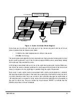
Page 38: ...MOTOROLA DSP96002 USER S MANUAL 3 15 Figure 3 4 Modulo Arithmetic Unit Block Diagram ...
Page 39: ...3 16 DSP96002 USER S MANUAL MOTOROLA ...
Page 53: ...4 14 DSP96002 USER S MANUAL MOTOROLA ...
Page 76: ...MOTOROLA DSP96002 USER S MANUAL 5 23 Figure 5 8 Address Modifier Summary ...
Page 86: ...6 10 DSP96002 USER S MANUAL MOTOROLA ...
Page 101: ...MOTOROLA DSP96002 USER S MANUAL 7 15 Figure 7 9 HI Block Diagram One Port ...
Page 140: ...7 54 DSP96002 USER S MANUAL MOTOROLA ...
Page 166: ...9 10 DSP96002 USER S MANUAL MOTOROLA ...
Page 181: ...MOTOROLA DSP96002 USER S MANUAL 10 15 Figure 10 8 Program Address Bus FIFO ...
Page 337: ...MOTOROLA DSP96002 USER S MANUAL A 149 ...
Page 404: ...A 216 DSP96002 USER S MANUAL MOTOROLA PC xxxx D ...
Page 460: ...A 272 DSP96002 USER S MANUAL MOTOROLA SIOP Not affected ...
Page 484: ...A 296 DSP96002 USER S MANUAL MOTOROLA SSH PC SSL SR SP 1 SP ...
Page 519: ...MOTOROLA DSP96002 USER S MANUAL A 331 ...
Page 718: ...MOTOROLA DSP96002 USER S MANUAL B 199 ...
Page 871: ... MOTOROLA INC 1994 MOTOROLA TECHNICAL DATA SEMICONDUCTOR M Addendum ...
Page 888: ...MOTOROLA INDEX 1 INDEX ...
Page 889: ......


