

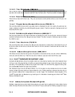


10 - 14
DSP96002 USER’S MANUAL
MOTOROLA
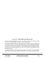
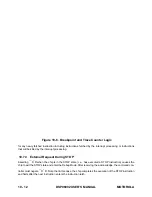
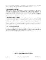
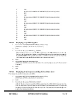
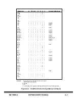
Figure 10-7. Pipeline Information Registers
through the serial interface. This register is affected by the operations performed during the Debug Mode
and must be restored by the command controller when returning to normal mode.
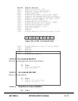
10.8.3
PIL Register (OPILR)
The PIL Register is a 32-bit latch that stores the value of the Instruction Latch before the Debug Mode is
entered. OPILR can only be read through the serial interface. This register is affected by the operations per-
formed during the Debug Mode and must be restored by the command controller when returning to normal
mode. Since there is no direct access to this register, this task is accomplished by writing the OPDBR first
and then the data from OPDBR is latched in OPILR.
10.8.4
GDB Register (OGDBR)
The GDB Register is a 32-bit latch that can only be read through the serial interface. OGDBR is not actually
required from a pipeline status restore point of view but is required as a means of passing information be-
tween the chip and the command controller. OGDBR is mapped on the X internal I/O space at address
$FFFFFFF0. Whenever the command controller needs a data word such as a register or memory value, it
will force the chip to execute an instruction that brings that information to OGDBR. Then, the contents of
OGDBR will be delivered serially to the command controller by the command "READ GDB REGISTER".
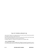
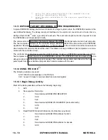
10.9
PAB HISTORY BUFFER
To ease the debugging activity and keep track of the program flow, a First-In-First-Out buffer is provided
which stores the addresses of the last five instructions that were executed as well as the addresses of the
last fetched instruction and of the instruction currently in the Instruction Latch.
Summary of Contents for DSP96002
Page 3: ...1 2 DSP96002 USER S MANUAL MOTOROLA ...
Page 38: ...MOTOROLA DSP96002 USER S MANUAL 3 15 Figure 3 4 Modulo Arithmetic Unit Block Diagram ...
Page 39: ...3 16 DSP96002 USER S MANUAL MOTOROLA ...
Page 53: ...4 14 DSP96002 USER S MANUAL MOTOROLA ...
Page 76: ...MOTOROLA DSP96002 USER S MANUAL 5 23 Figure 5 8 Address Modifier Summary ...
Page 86: ...6 10 DSP96002 USER S MANUAL MOTOROLA ...
Page 101: ...MOTOROLA DSP96002 USER S MANUAL 7 15 Figure 7 9 HI Block Diagram One Port ...
Page 140: ...7 54 DSP96002 USER S MANUAL MOTOROLA ...
Page 166: ...9 10 DSP96002 USER S MANUAL MOTOROLA ...
Page 181: ...MOTOROLA DSP96002 USER S MANUAL 10 15 Figure 10 8 Program Address Bus FIFO ...
Page 337: ...MOTOROLA DSP96002 USER S MANUAL A 149 ...
Page 404: ...A 216 DSP96002 USER S MANUAL MOTOROLA PC xxxx D ...
Page 460: ...A 272 DSP96002 USER S MANUAL MOTOROLA SIOP Not affected ...
Page 484: ...A 296 DSP96002 USER S MANUAL MOTOROLA SSH PC SSL SR SP 1 SP ...
Page 519: ...MOTOROLA DSP96002 USER S MANUAL A 331 ...
Page 718: ...MOTOROLA DSP96002 USER S MANUAL B 199 ...
Page 871: ... MOTOROLA INC 1994 MOTOROLA TECHNICAL DATA SEMICONDUCTOR M Addendum ...
Page 888: ...MOTOROLA INDEX 1 INDEX ...
Page 889: ......


