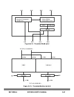
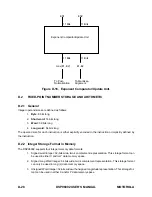


MOTOROLA
11
Locking a sector does not affect the contents of the cache sector (instructions already
fetched into the cache sector storage area), the valid-bits or the tag register contents of
that particular sector.
2.6.2
PRAM Mode
In the PRAM mode the DSP96002 is fully compatible with the original DSP96002. The in-
ternal program RAM is either enabled or disabled, according to the OMR. DMA references
to/from program memory, and the MOVEM instruction are fully enabled.
Nevertheless, when writing a word into the internal PRAM in PRAM mode, the corre-
sponding valid-bit is set, indicating that, when the user switches into cache mode, the
word has been initialized and is therefore valid.
In the PRAM mode, the processor does not update the tag registers in any way, it does
not update the SRU, it does not test the valid-bits, and it ignores the HIT/MISS signal.
The PFLUSH and PFREE instructions can be issued when the chip is in PRAM mode. For
further information on PFLUSH usage, refer to the next section.
2.6.3
Cache Flush
Cache flush is a cache operation rather than a cache operating mode. It is performed by
executing the PFLUSH instruction, which causes a global cache flush that brings the
cache to a reset condition. All valid-bits will be cleared. The tag registers’ values will form
a contiguous 1K segment of memory and therefore hold the values 0,1,2,...,7 that corre-
spond to the PRAM addresses 0, 128, 256,... etc. The LRU stack will hold a default de-
scending order of sectors. All locked cache sectors will be unlocked.
PFLUSH works in either PRAM or cache mode.
When switching from PRAM mode to cache mode, the PFLUSH instruction will allow the
user to flush the old data stored in the internal Program Memory. But if the user has
brought valid data into the internal program memory while in PRAM mode and would pre-
fer to leave the data untouched, it is not necessary to execute the PFLUSH instruction in
connection with changing modes.
However, when switching from cache mode to PRAM mode the cache is not flushed au-
tomatically and it is highly recommended that the PFLUSH instruction be executed. If the
cache is not flushed, the tag register could contain values different than the 0 to 1K ad-
dress mapping. In such a case, a write into the internal PRAM could set a valid-bit that
corresponds, from the tag value point of view, to an address outside the 0 to 1K address
range. This will be transparent to the user while in PRAM mode, but it could be harmful
when switching back to cache mode (again if no PFLUSH had been executed).
Summary of Contents for DSP96002
Page 3: ...1 2 DSP96002 USER S MANUAL MOTOROLA ...
Page 38: ...MOTOROLA DSP96002 USER S MANUAL 3 15 Figure 3 4 Modulo Arithmetic Unit Block Diagram ...
Page 39: ...3 16 DSP96002 USER S MANUAL MOTOROLA ...
Page 53: ...4 14 DSP96002 USER S MANUAL MOTOROLA ...
Page 76: ...MOTOROLA DSP96002 USER S MANUAL 5 23 Figure 5 8 Address Modifier Summary ...
Page 86: ...6 10 DSP96002 USER S MANUAL MOTOROLA ...
Page 101: ...MOTOROLA DSP96002 USER S MANUAL 7 15 Figure 7 9 HI Block Diagram One Port ...
Page 140: ...7 54 DSP96002 USER S MANUAL MOTOROLA ...
Page 166: ...9 10 DSP96002 USER S MANUAL MOTOROLA ...
Page 181: ...MOTOROLA DSP96002 USER S MANUAL 10 15 Figure 10 8 Program Address Bus FIFO ...
Page 337: ...MOTOROLA DSP96002 USER S MANUAL A 149 ...
Page 404: ...A 216 DSP96002 USER S MANUAL MOTOROLA PC xxxx D ...
Page 460: ...A 272 DSP96002 USER S MANUAL MOTOROLA SIOP Not affected ...
Page 484: ...A 296 DSP96002 USER S MANUAL MOTOROLA SSH PC SSL SR SP 1 SP ...
Page 519: ...MOTOROLA DSP96002 USER S MANUAL A 331 ...
Page 718: ...MOTOROLA DSP96002 USER S MANUAL B 199 ...
Page 871: ... MOTOROLA INC 1994 MOTOROLA TECHNICAL DATA SEMICONDUCTOR M Addendum ...
Page 888: ...MOTOROLA INDEX 1 INDEX ...
Page 889: ......


