


MOTOROLA
DSP96002 USER’S MANUAL
2 - 13
3:4.
When the Address and Memory Reference signals are stable, the data transfer is enabled by
the Transfer Strobe
—
T
–
S signal.
—
T
–
S is asserted to "qualify" the Address and Memory
Reference signals as stable and to perform the read or write data transfer.
—
T
–
S is asserted
in the second phase of the bus cycle.
3:5.
Wait states are inserted into the bus cycle controlled by a wait state counter or by
—
T
–
A,
whichever is longer. The wait state counter is loaded from the Bus Control Register. If the
wait state number determined by these two factors is zero, no wait states are inserted into
the bus cycle and
—
T
–
S is deasserted in the fourth phase. If the wait state number deter-
mined is W, then W wait states are inserted into the instruction cycle. Each wait state intro-
duces one Tc delay.
3:6.
When the Transfer Strobe
—
T
–
S is deasserted at the end of a bus cycle, the data is latched
in the destination device. At the end of a read cycle, the DSP96002 latches the data inter-
nally. At the end of a write cycle, the external memory latches the data. The Address signals
remain stable until the first phase of the next external bus cycle to minimize power dissipa-
tion. The Memory Reference signals S1 and S0 are deasserted during periods of no bus ac-
tivity and the data signals are three-stated.
3.6.1 Static RAM Support
Static RAM devices can be easily interfaced to the DSP96002 bus timing. There are two basic techniques
-
—
C
–
S controlled writes and
—
W
–
E controlled writes.
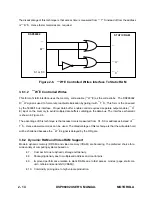
3. 6.1.1
—
C
–
S Controlled Writes
This form of static interface uses the memory chip select (
—
C
–
S) as the write strobe. The DSP96002 R/
—
W signal is used as an early read/write direction indication. Proper data buffer enable control on RAMs
without a separate output enable (
—
O
–
E) input must use this form to avoid multiple data buffers colliding
on the data bus. The interface schematic is shown in Figure 2-5.
Figure 2-5.
—
C
–
S Controlled Writes Interface to Static RAM
DSP96002
STATIC RAM
—
C
–
S
—
W
–
E
R/
—
W
—
T
–
Summary of Contents for DSP96002
Page 3: ...1 2 DSP96002 USER S MANUAL MOTOROLA ...
Page 38: ...MOTOROLA DSP96002 USER S MANUAL 3 15 Figure 3 4 Modulo Arithmetic Unit Block Diagram ...
Page 39: ...3 16 DSP96002 USER S MANUAL MOTOROLA ...
Page 53: ...4 14 DSP96002 USER S MANUAL MOTOROLA ...
Page 76: ...MOTOROLA DSP96002 USER S MANUAL 5 23 Figure 5 8 Address Modifier Summary ...
Page 86: ...6 10 DSP96002 USER S MANUAL MOTOROLA ...
Page 101: ...MOTOROLA DSP96002 USER S MANUAL 7 15 Figure 7 9 HI Block Diagram One Port ...
Page 140: ...7 54 DSP96002 USER S MANUAL MOTOROLA ...
Page 166: ...9 10 DSP96002 USER S MANUAL MOTOROLA ...
Page 181: ...MOTOROLA DSP96002 USER S MANUAL 10 15 Figure 10 8 Program Address Bus FIFO ...
Page 337: ...MOTOROLA DSP96002 USER S MANUAL A 149 ...
Page 404: ...A 216 DSP96002 USER S MANUAL MOTOROLA PC xxxx D ...
Page 460: ...A 272 DSP96002 USER S MANUAL MOTOROLA SIOP Not affected ...
Page 484: ...A 296 DSP96002 USER S MANUAL MOTOROLA SSH PC SSL SR SP 1 SP ...
Page 519: ...MOTOROLA DSP96002 USER S MANUAL A 331 ...
Page 718: ...MOTOROLA DSP96002 USER S MANUAL B 199 ...
Page 871: ... MOTOROLA INC 1994 MOTOROLA TECHNICAL DATA SEMICONDUCTOR M Addendum ...
Page 888: ...MOTOROLA INDEX 1 INDEX ...
Page 889: ......


