


2 - 14
DSP96002 USER’S MANUAL
MOTOROLA
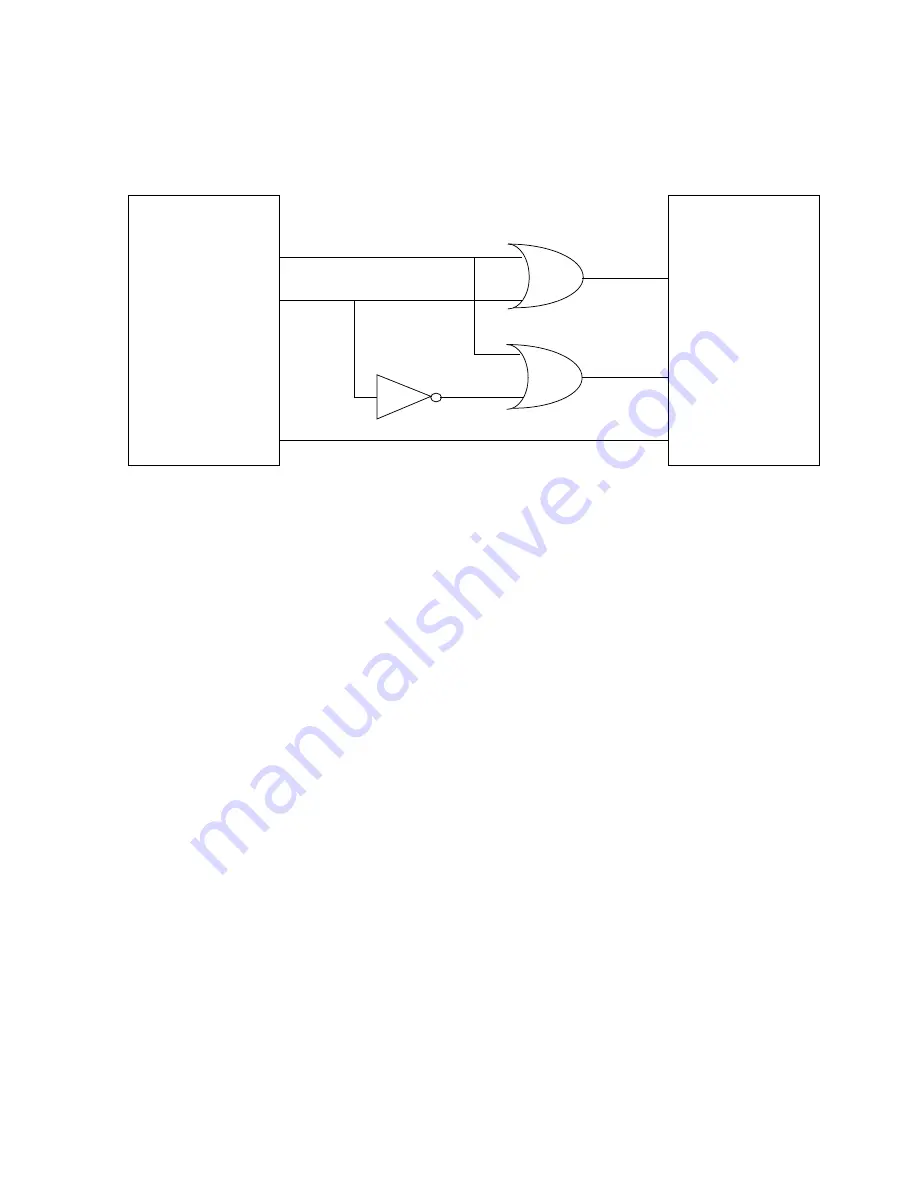
3. 6.1.2
—
W
–
E Controlled Writes
This form of static interface uses the memory write enable (
—
W
–
E) as the write strobe. The DSP96002
R/
—
W signal is used to form a late read/write indication by gating it with
—
T
–
S. This form is the one used
by the 56000/1 bus interface. Proper data buffer enable control requires a separate output enable (
—
O
–
E) input on the memory to avoid multiple data buffers colliding on the data bus. The interface schematic
is shown in Figure 2-6.
The advantage of this technique is that access time is measured from S1, S0 or addresses instead of
—
T
–
S. Hence slower memories can be used. The disadvantage of this technique is that the write data hold
will be shortened because the
—
W
–
E signal is delayed by the OR gate.
3.6.2 Dynamic RAM and Video RAM Support
Modern dynamic memory (DRAM) and video memory (VRAM) are becoming the preferred choice for a
wide variety of computing systems based on
4:7.
Cost per bit due to dynamic storage cell density.
4:8.
Packaging density due to multiplexed address and control pins.
4:9.
Improved performance relative to static RAMs due to fast access modes (page, static col-
umn, nibble and serial shift (VRAM)).
4:10. Commodity pricing due to high volume production.
DSP96002
—
R/
—
STATIC RAM
—
—
O
–
—
C
–
S1 or S0
Figure 2-6.
—
W
–
E Controlled Writes Interface To Static RAM
The disadvantage of this technique is that access time is measured from
—
T
–
S instead of from the address
or
—
B
–
S. Hence faster memories are required.
Summary of Contents for DSP96002
Page 3: ...1 2 DSP96002 USER S MANUAL MOTOROLA ...
Page 38: ...MOTOROLA DSP96002 USER S MANUAL 3 15 Figure 3 4 Modulo Arithmetic Unit Block Diagram ...
Page 39: ...3 16 DSP96002 USER S MANUAL MOTOROLA ...
Page 53: ...4 14 DSP96002 USER S MANUAL MOTOROLA ...
Page 76: ...MOTOROLA DSP96002 USER S MANUAL 5 23 Figure 5 8 Address Modifier Summary ...
Page 86: ...6 10 DSP96002 USER S MANUAL MOTOROLA ...
Page 101: ...MOTOROLA DSP96002 USER S MANUAL 7 15 Figure 7 9 HI Block Diagram One Port ...
Page 140: ...7 54 DSP96002 USER S MANUAL MOTOROLA ...
Page 166: ...9 10 DSP96002 USER S MANUAL MOTOROLA ...
Page 181: ...MOTOROLA DSP96002 USER S MANUAL 10 15 Figure 10 8 Program Address Bus FIFO ...
Page 337: ...MOTOROLA DSP96002 USER S MANUAL A 149 ...
Page 404: ...A 216 DSP96002 USER S MANUAL MOTOROLA PC xxxx D ...
Page 460: ...A 272 DSP96002 USER S MANUAL MOTOROLA SIOP Not affected ...
Page 484: ...A 296 DSP96002 USER S MANUAL MOTOROLA SSH PC SSL SR SP 1 SP ...
Page 519: ...MOTOROLA DSP96002 USER S MANUAL A 331 ...
Page 718: ...MOTOROLA DSP96002 USER S MANUAL B 199 ...
Page 871: ... MOTOROLA INC 1994 MOTOROLA TECHNICAL DATA SEMICONDUCTOR M Addendum ...
Page 888: ...MOTOROLA INDEX 1 INDEX ...
Page 889: ......


