


DS33Z41 Quad IMUX Ethernet Mapper
104 of 167
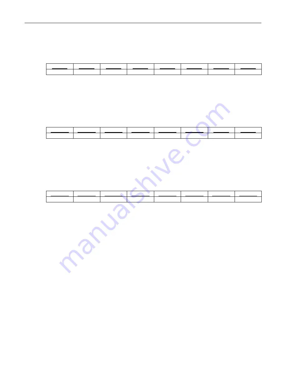
Register Name:
LI.RFPCB0
Register Description:
Receive FCS Errored Packet Count Byte 0 Register
Register Address:
10Ch
Bit
# 7 6 5 4 3 2 1 0
Name RFPC7 RFPC6 RFPC5 RFPC4 RFPC3 RFPC2 RFPC1 RFPC0
Default
0 0 0 0 0 0 0 0
Bits 7 to 0: Receive FCS Errored Packet Count (RFPC7 to RFPC0).
Eight bits of a 24-bit value. Register
description below.
Register Name:
LI.RFPCB1
Register Description:
Receive FCS Errored Packet Count Byte 1 Register
Register Address:
10Dh
Bit
# 7 6 5 4 3 2 1 0
Name RFPC15 RFPC14 RFPC13 RFPC12 RFPC11 RFPC10 RFPC9 RFPC8
Default
0 0 0 0 0 0 0 0
Bits 7 to 0: Receive FCS Errored Packet Count (RFPC15 to RFPC8).
Eight bits of a 24-bit value. Register
description below.
Register Name:
LI.RFPCB2
Register Description:
Receive FCS Errored Packet Count Byte 2 Register
Register Address:
10Eh
Bit
# 7 6 5 4 3 2 1 0
Name RFPC23 RFPC22 RFPC21 RFPC20 RFPC19 RFPC18 RFPC17 RFPC16
Default
0 0 0 0 0 0 0 0
Bits 7 to 0: Receive FCS Errored Packet Count (RFPC23 to RFPC16).
These 24 bits indicate the number of
packets received with an FCS error. The byte count for these packets is included in the receive aborted byte
count register REBCR.