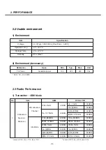
2. PERFORMANCE
- 10 -
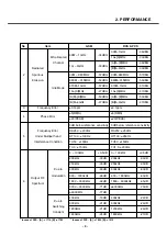
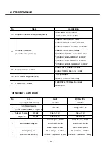
No
Item
GSM
DCS & PCS
Frequency offset
800kHz
7
Intermodulation attenuation
–
Intermodulation product should
be Less than 55dB below the
level of Wanted signal
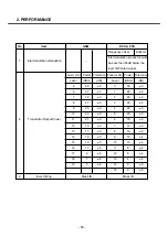
Power control Power Tolerance Power control Power Tolerance
Level
(dBm)
(dB)
Level
(dBm)
(dB)
5
33
±3
0
30
±3
6
31
±3
1
28
±3
7
29
±3
2
26
±3
8
27
±3
3
24
±3
9
25
±3
4
22
±3
10
23
±3
5
20
±3
8
Transmitter Output Power
11
21
±3
6
18
±3
12
19
±3
7
16
±3
13
17
±3
8
14
±3
14
15
±3
9
12
±4
15
13
±3
10
10
±4
16
11
±5
11
8
±4
17
9
±5
12
6
±4
18
7
±5
13
4
±4
19
5
±5
14
2
±5
15
0
±5
9
Burst timing
Mask IN
Mask IN
Summary of Contents for U8500
Page 1: ...Date February 2006 Issue 1 0 Service Manual Model U8500 Service Manual U8500 ...
Page 20: ...3 TECHNICAL BRIEF 21 ...
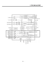
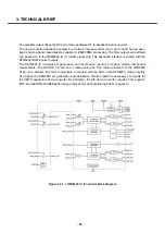
Page 32: ...3 TECHNICAL BRIEF 33 Figure 3 5 6 1 GSM PA functional block diagram ...
Page 35: ...3 TECHNICAL BRIEF 36 Figure 3 5 10 1 Bluetooth system architecture ...
Page 50: ...3 TECHNICAL BRIEF 51 Figure 3 10 3 2 1 PM6650 Functional Block Diagram ...
Page 114: ...4 TROUBLE SHOOTING 115 Loud Speaker U502 U503 Amp ...
Page 118: ...4 TROUBLE SHOOTING 119 C200 C201 for MIC serial capacitor ...
Page 121: ...4 TROUBLE SHOOTING 122 Q404 Q403 Q402 VBATT GND ...
Page 143: ...6 BLOCK DIAGRAM 144 6 3 Interface Diagram U8500 Interface Diagram ...
Page 145: ... 146 ...
Page 154: ... 155 U8500 8 PCB LAYOUT ...
Page 155: ... 156 8 PCB LAYOUT U8500 ...
Page 156: ... 157 8 PCB LAYOUT ...
Page 157: ... 158 8 PCB LAYOUT ...
Page 158: ... 159 U8500 8 PCB LAYOUT ...
Page 159: ... 160 U8500 8 PCB LAYOUT ...
Page 166: ...9 CALIBRATION 167 Click START button U8500 U8500_ver1 1 U8500 U8500 Click U8500 ...
Page 167: ... 168 ...
Page 169: ... 170 ...
Page 194: ...Note ...
Page 195: ...Note ...


