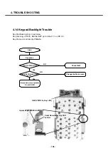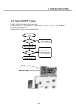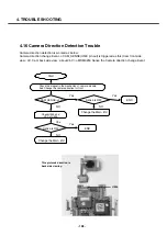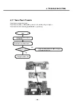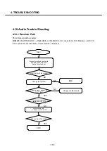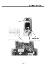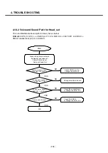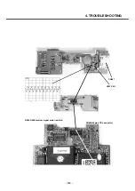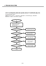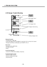
4.19 Charger Trouble Shooting
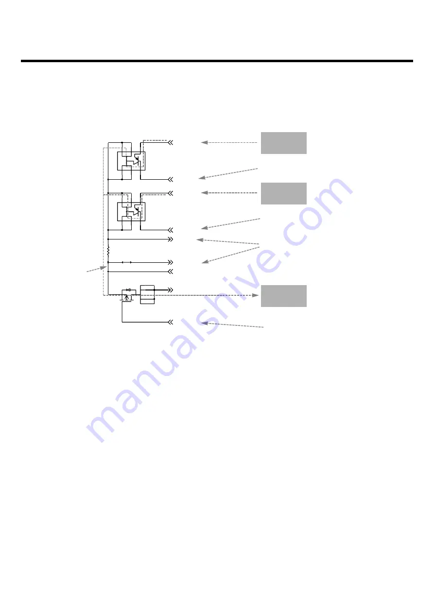
Charging Procedure
- Connecting TA or USB Cable
- Control the charging current by PM6050 IC using USB_CNT_N or CHG_CNT_N signal
- Charging Current flows into the battery by control BATT_FET_N
Check Point
- Connection of TA or USB Cable
- Charging current path
- Battery
Trouble Shooting Setup
- Connect TA or USB Cable and battery to the phone
Trouble Shooting Procedure
- Check the charger connector
- Check the charging current Path
- Check the battery
4. TROUBLE SHOOTING
- 120 -
B
3
C1
1
2
C2
5
6
4
QST4
Q404
0.1
R409
Q403
QST4
3 B
1
C1
C2
2
5
6
4
G
S
D1
D2
D3
D4
SI3493DV-E3
Q402
+VPWR
USB_VBUS
ICHARGE
+5V_PWR
USB_CNT_N
CHG_CNT_N
VBATT
BATT_FET_N
ICHARGEOUT
Pass control Tr
(ON)
USB Charging control
USB Cable
(5.0V)
Pass control Tr
(ON)
Battery FET
(ON)
4.2~4.25V
TA
(4.6V)
Main
Battery
TA Charging control
Charging current sensing
Battery charging control
Summary of Contents for U8500
Page 1: ...Date February 2006 Issue 1 0 Service Manual Model U8500 Service Manual U8500 ...
Page 20: ...3 TECHNICAL BRIEF 21 ...
Page 32: ...3 TECHNICAL BRIEF 33 Figure 3 5 6 1 GSM PA functional block diagram ...
Page 35: ...3 TECHNICAL BRIEF 36 Figure 3 5 10 1 Bluetooth system architecture ...
Page 50: ...3 TECHNICAL BRIEF 51 Figure 3 10 3 2 1 PM6650 Functional Block Diagram ...
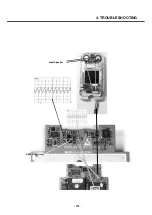
Page 114: ...4 TROUBLE SHOOTING 115 Loud Speaker U502 U503 Amp ...
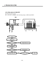
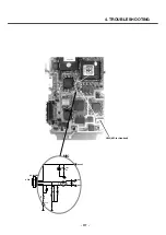
Page 118: ...4 TROUBLE SHOOTING 119 C200 C201 for MIC serial capacitor ...
Page 121: ...4 TROUBLE SHOOTING 122 Q404 Q403 Q402 VBATT GND ...
Page 143: ...6 BLOCK DIAGRAM 144 6 3 Interface Diagram U8500 Interface Diagram ...
Page 145: ... 146 ...
Page 154: ... 155 U8500 8 PCB LAYOUT ...
Page 155: ... 156 8 PCB LAYOUT U8500 ...
Page 156: ... 157 8 PCB LAYOUT ...
Page 157: ... 158 8 PCB LAYOUT ...
Page 158: ... 159 U8500 8 PCB LAYOUT ...
Page 159: ... 160 U8500 8 PCB LAYOUT ...
Page 166: ...9 CALIBRATION 167 Click START button U8500 U8500_ver1 1 U8500 U8500 Click U8500 ...
Page 167: ... 168 ...
Page 169: ... 170 ...
Page 194: ...Note ...
Page 195: ...Note ...

