3. TECHNICAL BRIEF
- 35 -
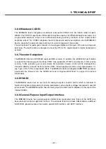
3.5.9 VCTCXO (X1000)
The Voltage Controlled Temperature Compensated Crystal Oscillator (VCTCXO) provides the
reference frequency for all RFIC synthesizers as well as clock generation functions within the
MSM6250 IC. The 6250-series chipset requires a 19.2 MHz nominal VCTCXO frequency. The
oscillator frequency is controlled by the MSM6250’s TRK_LO_ADJ pulse density modulated signal in
the same manner as the transmit gain control.
The filtered PDM signal results in an analog control signal into the VCTCXO tuning port whose voltage
is directly proportional to the density of the digital bit stream. The MSM device varies the pulse density
to change the analog control voltage that sets the oscillator frequency - all within a feedback control
loop that minimizes handset frequency drift relative to the network.
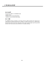
3.5.10 Bluetooth (U406 : LBDA254AN0, ANT400 : LDA31 )
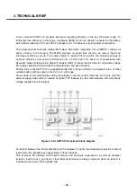
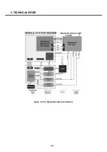
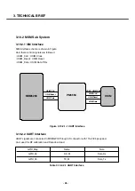
The MSM6250 includes BT baseband embedded BT 1.1 compliant baseband core, so the other
bluetooth components are an bluetooth RF module and Antenna. Figure1.5.12-1 shows the bluetooth
system architecture in the U8500.
Summary of Contents for U8500
Page 1: ...Date February 2006 Issue 1 0 Service Manual Model U8500 Service Manual U8500 ...
Page 20: ...3 TECHNICAL BRIEF 21 ...
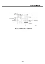
Page 32: ...3 TECHNICAL BRIEF 33 Figure 3 5 6 1 GSM PA functional block diagram ...
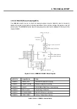
Page 35: ...3 TECHNICAL BRIEF 36 Figure 3 5 10 1 Bluetooth system architecture ...
Page 50: ...3 TECHNICAL BRIEF 51 Figure 3 10 3 2 1 PM6650 Functional Block Diagram ...
Page 114: ...4 TROUBLE SHOOTING 115 Loud Speaker U502 U503 Amp ...
Page 118: ...4 TROUBLE SHOOTING 119 C200 C201 for MIC serial capacitor ...
Page 121: ...4 TROUBLE SHOOTING 122 Q404 Q403 Q402 VBATT GND ...
Page 143: ...6 BLOCK DIAGRAM 144 6 3 Interface Diagram U8500 Interface Diagram ...
Page 145: ... 146 ...
Page 154: ... 155 U8500 8 PCB LAYOUT ...
Page 155: ... 156 8 PCB LAYOUT U8500 ...
Page 156: ... 157 8 PCB LAYOUT ...
Page 157: ... 158 8 PCB LAYOUT ...
Page 158: ... 159 U8500 8 PCB LAYOUT ...
Page 159: ... 160 U8500 8 PCB LAYOUT ...
Page 166: ...9 CALIBRATION 167 Click START button U8500 U8500_ver1 1 U8500 U8500 Click U8500 ...
Page 167: ... 168 ...
Page 169: ... 170 ...
Page 194: ...Note ...
Page 195: ...Note ...

