3. TECHNICAL BRIEF
- 40 -
3.8 Subsystem(MSM6250)
3.8.1 ARM Microprocessor Subsystem
The MSM6250 device uses an embedded ARM926EJ-S microprocessor. This microprocessor,
through the system software, controls most of the functionality for the MSM, including control of the
external peripherals such as the keypad, LCD, RAM, and ROM devices. Through a QUALCOMM
proprietary serial bus interface (SBI) the ARM926EJ-S configures and controls the functionality of the
RTR6250, RFR6200, RFL6200, and PM6650 devices.
3.8.2 UMTS Subsystem
The UMTS Subsystem performs the digital UMTS signal processing. Its components include:
• Searcher engine
• Demodulating fingers
• Combining block
• Frame deinterleaver
• Viterbi decoder
• Up-link subsystem
• Turbo decoder
On the down-link channel the UMTS subsystem searches, demodulates, and decodes incoming
CPICH, CCPCH, SCH, and Traffic Channel information. It extracts packet data from the downlink
traffic channel and prepares the packet data for processing. For the up-link, the CDMA subsystem
processes the packet data and modulates the up-link traffic channel (DCH).
3.8.3 GSM Subsystem
The GSM Subsystem performs the digital GSM signal processing.
3.8.4 RF Interface
The RF interface communicates with the mobile station’s external RF and analog baseband circuits.
Signals to these circuits control signal gain in the Rx and Tx signal path and maintain The system’s
frequency reference.
3.8.5 Serial Bus Interface(SBI)
The MSM6250 device’s SBI is designed specifically to be a quick, low pin count control protocol for
QUALCOMM’s RTR6250, RFR6200, RFL6200, and PM6650 ASICs. Using the SBI, the RTR6250,
RFR6200, RFL6200, and PM6650 devices can be configured for different operating modes and for
minimum power consumption, extending battery life in Standby mode. The SBI also controls DC
baseband offset errors.
Summary of Contents for U8500
Page 1: ...Date February 2006 Issue 1 0 Service Manual Model U8500 Service Manual U8500 ...
Page 20: ...3 TECHNICAL BRIEF 21 ...
Page 32: ...3 TECHNICAL BRIEF 33 Figure 3 5 6 1 GSM PA functional block diagram ...
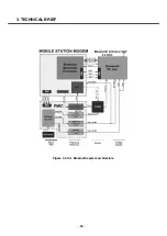
Page 35: ...3 TECHNICAL BRIEF 36 Figure 3 5 10 1 Bluetooth system architecture ...
Page 50: ...3 TECHNICAL BRIEF 51 Figure 3 10 3 2 1 PM6650 Functional Block Diagram ...
Page 114: ...4 TROUBLE SHOOTING 115 Loud Speaker U502 U503 Amp ...
Page 118: ...4 TROUBLE SHOOTING 119 C200 C201 for MIC serial capacitor ...
Page 121: ...4 TROUBLE SHOOTING 122 Q404 Q403 Q402 VBATT GND ...
Page 143: ...6 BLOCK DIAGRAM 144 6 3 Interface Diagram U8500 Interface Diagram ...
Page 145: ... 146 ...
Page 154: ... 155 U8500 8 PCB LAYOUT ...
Page 155: ... 156 8 PCB LAYOUT U8500 ...
Page 156: ... 157 8 PCB LAYOUT ...
Page 157: ... 158 8 PCB LAYOUT ...
Page 158: ... 159 U8500 8 PCB LAYOUT ...
Page 159: ... 160 U8500 8 PCB LAYOUT ...
Page 166: ...9 CALIBRATION 167 Click START button U8500 U8500_ver1 1 U8500 U8500 Click U8500 ...
Page 167: ... 168 ...
Page 169: ... 170 ...
Page 194: ...Note ...
Page 195: ...Note ...


