3.5.6 Dual band GSM power amplifier (U1005)
The SKY77328 Power Amplifier Module (PAM) is designed in a low profile (1.2mm), compact form
factor for quad-band cellular handsets comprising GSM850/900, DCS1800, and PCS1900 operation.
The PAM also supports Class 12 General Packet Radio Service (GPRS) multi-slot operation.
The module consists of separate GSM850/900 PA and DCS1800/PCS1900 PA blocks, impedance-
matching circuitry for 50 Ω input and output impedances, and a Power Amplifier Control (PAC) block
with an internal current-sense resistor. The custom BiCMOS integrated circuit provides the internal
PAC function and interface circuitry.
Fabricated onto a single Gallium Arsenide (GaAs) die, one Heterojunction Bipolar Transistor (HBT) PA
block supports the GSM850/900 bands and the other supports the DCS1800 and PCS1900 bands.
Both PA blocks share common power supply pins to distribute current. The GaAs die, the Silicon (Si)
die, and the passive components are mounted on a multi-layer laminate substrate. The assembly is
encapsulated with plastic overmold.
RF input and output ports of the SKY77328 are internally matched to a 50 Ω load to reduce the
number of external components for a quad-band design.
Extremely low leakage current (2.5 µA, typical) of the dual PA module maximizes handset standby
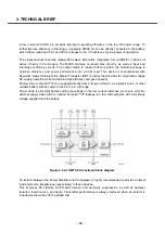
time. The SKY77328 also contains band-select switching circuitry to select GSM (logic 0) or DCS/PCS
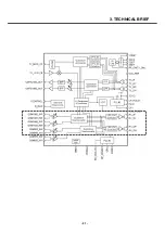
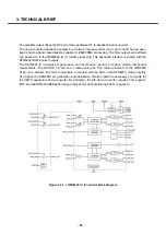
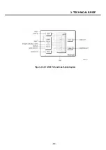
(logic 1) as determined from the Band Select (BS) signal. In Figure 1.5.6-1 below, the BS pin selects
the PA output (DCS/PCS OUT or GSM850/900 OUT) and the Analog Power Control (VAPC) controls
the level of output power.
The VBATT pin connects to an internal current-sense resistor and interfaces to an integrated power
amplifier control (iPAC™) function, which is insensitive to variations in temperature, power supply,
process, and input power. The ENABLE input allows initial turn-on of PAM circuitry to minimize battery
drain.
3. TECHNICAL BRIEF
- 32 -
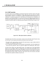
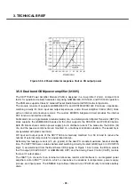
Figure 3.5.5-2 Power detector response, Vout vs PA output power
Summary of Contents for U8500
Page 1: ...Date February 2006 Issue 1 0 Service Manual Model U8500 Service Manual U8500 ...
Page 20: ...3 TECHNICAL BRIEF 21 ...
Page 32: ...3 TECHNICAL BRIEF 33 Figure 3 5 6 1 GSM PA functional block diagram ...
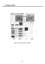
Page 35: ...3 TECHNICAL BRIEF 36 Figure 3 5 10 1 Bluetooth system architecture ...
Page 50: ...3 TECHNICAL BRIEF 51 Figure 3 10 3 2 1 PM6650 Functional Block Diagram ...
Page 114: ...4 TROUBLE SHOOTING 115 Loud Speaker U502 U503 Amp ...
Page 118: ...4 TROUBLE SHOOTING 119 C200 C201 for MIC serial capacitor ...
Page 121: ...4 TROUBLE SHOOTING 122 Q404 Q403 Q402 VBATT GND ...
Page 143: ...6 BLOCK DIAGRAM 144 6 3 Interface Diagram U8500 Interface Diagram ...
Page 145: ... 146 ...
Page 154: ... 155 U8500 8 PCB LAYOUT ...
Page 155: ... 156 8 PCB LAYOUT U8500 ...
Page 156: ... 157 8 PCB LAYOUT ...
Page 157: ... 158 8 PCB LAYOUT ...
Page 158: ... 159 U8500 8 PCB LAYOUT ...
Page 159: ... 160 U8500 8 PCB LAYOUT ...
Page 166: ...9 CALIBRATION 167 Click START button U8500 U8500_ver1 1 U8500 U8500 Click U8500 ...
Page 167: ... 168 ...
Page 169: ... 170 ...
Page 194: ...Note ...
Page 195: ...Note ...

