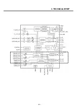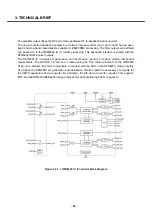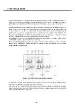
A generic, high-level functional block diagram of U8500 is shown in Figure 1-1. One antenna collects
base station forward link signals and radiates handset reverse link signals. The antenna connects with
receive and transmit paths through a switch module (plus a duplexer for UMTS-2100 operation).
UMTS band signals at the antenna are switched to the relevant UMTS duplexer.
The UMTS receive band signals are amplified by the front-end LNAs of the RFR6250 IC before
passing through a band-pass filter and being applied to the mixer inputs of the RFR6250 IC. On-chip
circuits down-convert the received signal directly from RF to baseband using radioOne Zero-IF
techniques. Generation and distribution of the UMTS LO, for the down-converter, is performed entirely
on-chip (except for the loop filter).
The RFR6250 IC outputs analog baseband signals for processing by the MSM device. This baseband
interface is shared with the RTR6250 GSM receiver outputs, but is separate from the GPS baseband
interface.
EGSM, DCS and PCS receive signals from the antenna switch module pass through their band-pass
filters, then are applied to the RTR6250 IC. In a similar fashion to the UMTS paths, RTR6250 IC
circuits down-convert the received signals directly from RF to baseband.
The GSM LO for multiband down conversion is entirely generated within the RTR6250 IC (PLL and
distribution functions) with exception of the off-chip loop filter. The RTR analog baseband outputs are
routed to the MSM6250 IC for further processing (an interface shared with the RFR UMTS receive
paths).
The UMTS transmit path begins with analog baseband signals from the MSM device that drive the
RTR6250 IC. Integrated PLL and VCO circuits generate the Tx LO used in the quadrature upconverter
that translates baseband signals directly to RF. The RTR6250 output driver stages deliver fairly high-
level signals that are filtered and applied to the power amplifiers (PA). The PA output is routed to the
antenna through a duplexer and switch module.
The shared EGSM-900, DCS-1800, and PCS-1900 transmit path begins with the same baseband
interface from the MSM6250 IC that is used for the UMTS band. A single EGSM/DCS/PCS quadrature
upconverter translates the GMSK-modulated signal to a convenient intermediate frequency (IF) that
forms one input to an offset phase-locked loop (OPLL).
OPLL functions are split between the RTR6250 IC and off-chip loop filter and dual Tx VCO circuits,
and translate the GMSK-modulated signal to the desired EGSM-900, DCS-1800 or PCS-1900 channel
frequency. This signal is applied to a dual power amplifier (only one is active at a time).
The enabled path continues with the PA, an automated power control (APC) circuit that samples the
transmit power and adjusts its level, the switch module (which includes a band-appropriate lowpass
filter), and the antenna.
3. TECHNICAL BRIEF
- 18 -
Summary of Contents for U8500
Page 1: ...Date February 2006 Issue 1 0 Service Manual Model U8500 Service Manual U8500 ...
Page 20: ...3 TECHNICAL BRIEF 21 ...
Page 32: ...3 TECHNICAL BRIEF 33 Figure 3 5 6 1 GSM PA functional block diagram ...
Page 35: ...3 TECHNICAL BRIEF 36 Figure 3 5 10 1 Bluetooth system architecture ...
Page 50: ...3 TECHNICAL BRIEF 51 Figure 3 10 3 2 1 PM6650 Functional Block Diagram ...
Page 114: ...4 TROUBLE SHOOTING 115 Loud Speaker U502 U503 Amp ...
Page 118: ...4 TROUBLE SHOOTING 119 C200 C201 for MIC serial capacitor ...
Page 121: ...4 TROUBLE SHOOTING 122 Q404 Q403 Q402 VBATT GND ...
Page 143: ...6 BLOCK DIAGRAM 144 6 3 Interface Diagram U8500 Interface Diagram ...
Page 145: ... 146 ...
Page 154: ... 155 U8500 8 PCB LAYOUT ...
Page 155: ... 156 8 PCB LAYOUT U8500 ...
Page 156: ... 157 8 PCB LAYOUT ...
Page 157: ... 158 8 PCB LAYOUT ...
Page 158: ... 159 U8500 8 PCB LAYOUT ...
Page 159: ... 160 U8500 8 PCB LAYOUT ...
Page 166: ...9 CALIBRATION 167 Click START button U8500 U8500_ver1 1 U8500 U8500 Click U8500 ...
Page 167: ... 168 ...
Page 169: ... 170 ...
Page 194: ...Note ...
Page 195: ...Note ...

