REL0.1
Page 86 of 95
Kintex Ult FPGA (KU19P) SOM Hardware User Guide
iWave Systems Technologies Pvt. Ltd.
3.1.2
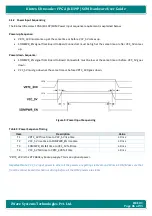
Power Input Sequencing
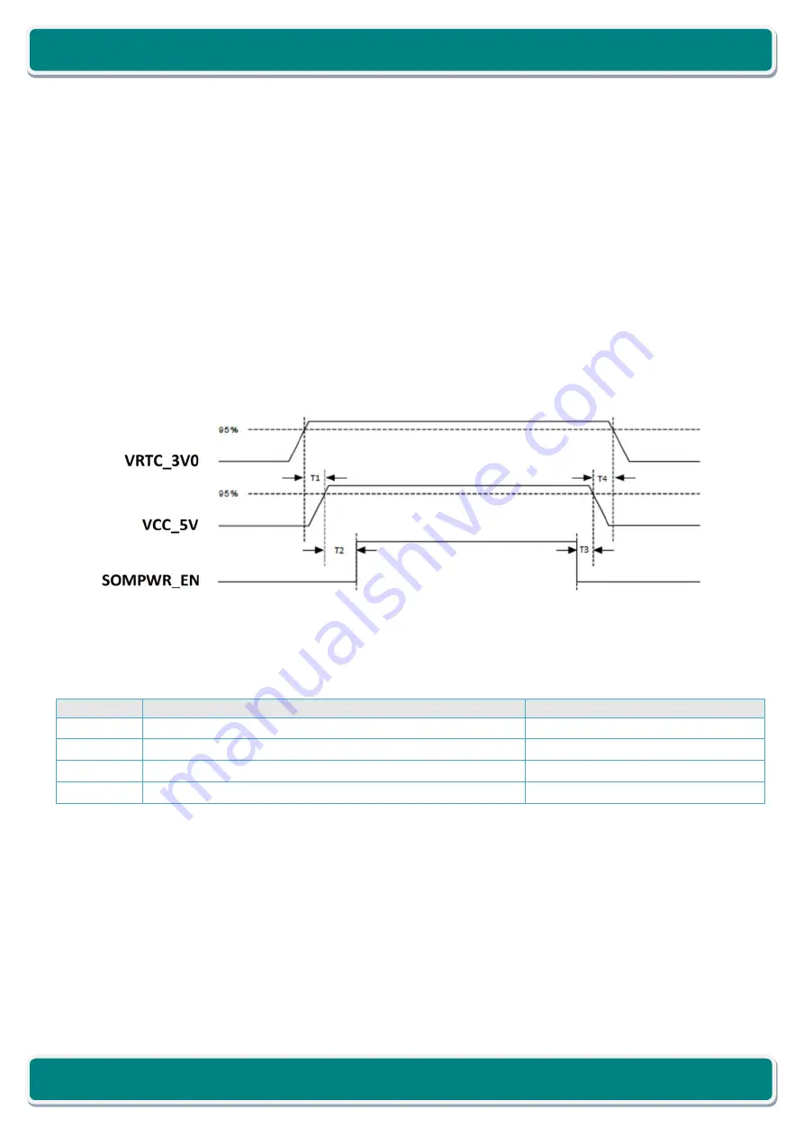
The Kintex Ult FPGA (KU19P) SOM Power Input sequence requirement is explained below.
Power up Sequence:
•
VRTC_3V0 must come up at the same time or before VCC_5V comes up.
•
SOMPWR_EN signal from Board to Board Connector1 must be high at the same time or after VCC_5V comes
up.
Power down Sequence:
•
SOMPWR_EN signal from Board to Board Connector1 must be low at the same time or before VCC_5V goes
down.
•
VCC_5V must go down at the same time or before VRTC_3V0 goes down.
Figure 9: Power Input Sequencing
Table 9: Power Sequence Timing
Item
Description
Value
T1
VRTC_3V0¹ rise time to VCC_5V rise time
≥ 0 ms
T2
VCC_5V rise time to SOMPWR_EN rise time
≥ 0 ms
T3
SOMPWR_EN fall time to VCC_5V fall time
≥ 0 ms
T4
VCC_5V fall time to VRTC_3V0 fall time
≥ 0 ms
¹ VRTC_3V0 is the RTC Battery backup supply. This is an optional power.
Important Note:
VCC_5V input power to other all the powers are getting stable around 50ms in SOM, Make sure that
from the carrier board IOs shall not driving before all the SOM powers are stable.

