REL0.1
Page 20 of 95
Kintex Ult FPGA SOM Hardware User Guide
iWave Systems Technologies Pvt. Ltd.
2.4
Layerscape Processor
2.4.1
Processor & Design Information
The Kintex Ult FPGA (KU19P) SOM is based on Xilinx Kintex Ult FPGA (KU19P) integrated with LS1021A
Layerscape Processor. Featuring a pair of extremely power-efficient 32-bit Arm Cortex-A7 cores with ECC protected L1 and L2
cache memories for high reliability, running up to 1.2 GHz, and providing pre-silicon CoreMark performance of over 5,000, the
LS102xA family delivers greater performance than any previous sub-4W communication processor. The Block Diagram of LS1021A
from NXP website is shown below for reference.
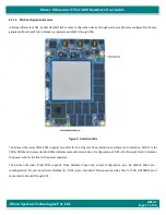
Figure 4: LS1021A Internal Block Diagram
2.4.1.1
LS1021A Booting and Configuration
The Kintex Ult SOM integrates KU19P FPGA SoC with L1021A Layerscape processor. The RCW and U-boot is programmed
in to the NOR Flash. On POR, Pre-Boot Loader (PBL) will fetch RCW configuration and PBL commands from NOR flash (chosen by
rcw_src selection pins). Then executes u-boot from NOR flash.


