REL0.1
Page 21 of 95
Kintex Ult FPGA SOM Hardware User Guide
iWave Systems Technologies Pvt. Ltd.
2.4.1.2
LS1021A PMIC
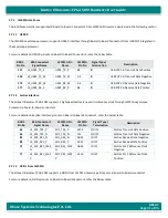
The Kintex Ult FPGA SOM supports Dialog semiconductor DA9062 PMIC and one regulator for LS1021A Processor. The
I2C2 module of LS1021A is used for PMIC interface through LS1021A pins with I2C address 0x58.
PMIC supports reset output and connected to LS1021A (LS_PMIC_POR) for power on reset. Also, PMIC supports IRQ output for
events indication and connected to
LS1021A’s
GPIO (GPIO3_23).
The PMIC supports Real Time Clock functionality. It uses the Coin cell battery power from Board-to-Board Connector2 pin68 for
RTC backup power. The PMIC can support backup battery charging to charge Lithium-Manganese coin cell batteries and super
capacitors if required.
2.4.1.3
LS1021A Reference Clock
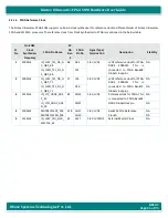
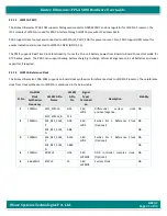
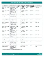
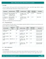
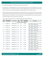
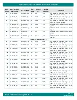
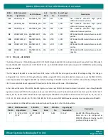
The Kintex Ult FPGA SOM supports on board clock synthesizer for reference clock to LS1021A Processor. These reference
clock from clock synthesizer to LS1021A is mentioned in the below table.
Sl. No
On-SOM
Clock
Synthesizer
Frequency
LS1021A Pin
Name
LS1021
A Pin
No
Signal
Type/
Terminati
on
Description
Stability
1
100MHz
DIFF_SYSCLK
G14
1.8V,
LVDS
Differential
system
clock
positive/negative.
NA
DIFF_SYSCLK_B
F14
2
100MHz
SD1_REF_CLK1_
P
AC8
1.8V,
LVDS
SerDes PLL 1 Reference Clock
(Optional)
NA
SD1_REF_CLK1_
N
AB8
NA
3
100MHz
SD1_REF_CLK2_
P
AC16
1.8V,
LVDS
SerDes PLL 2 Reference Clock
(Optional)
NA
SD1_REF_CLK2_
N
AB16
NA
4
100MHz
DDRCLK
H18
1.8V,
LVCMOS
DDR controller complex clock.
(Optional)
NA
5
66.66MHz
SYSCLK
F5
1.8V,
LVCMOS
System Clock
NA

