REL0.1
Page 10 of 95
Kintex Ult FPGA SOM Hardware User Guide
iWave Systems Technologies Pvt. Ltd.
2.
ARCHITECTURE AND DESIGN
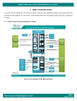
This section provides detailed information about the Kintex Ult FPGA (KU19P) SOM features and Hardware architecture
with high level block diagram. Also, this section provides detailed information about Board-to-Board connectors pin assignment
and usage.
2.1
Kintex Ult FPGA (KU19P) SOM Block Diagram
Kintex Ult KU19P FPGA (B2104) SOM Block Diagram
Board to Board
High Speed
Connector2
(240Pin)
Board to Board
High Speed
Connector1
(240Pin)
Kintex Ult
KU19P (B2104)
Dual Arm® Cortex®-A7 CPU
PCIe 2.0 x1
G
TY
T
ra
n
sc
ei
ver
DDR4
Controller
Ethernet1
Ethernet
PHY
Gigabit Ethernet
RGMII
USB1
USB 2.0 x 1
I2C x 2
Board to Board
High Speed
Connector3
(240Pin)
Board to Board
High Speed
Connector4
(80Pin)
FP
G
A
IO
s
DDR4
(64bit, 8bit ECC)
Bank
69,70, 71
DDR4
–
4GB
Bank
72,73,74
DDR4
–
4GB
Bank
228[2:0]
229,
230,
231,
232
G
TY
Tra
n
sc
ei
ver
Bank
225,
226
Bank
227
Bank
65, 67, 92
Bank 66,67
FP
G
A
I
O
s
High Speed Transceiver (8 Channels)
High Speed Transceiver (4 Channels)
High Speed Transceiver (19 Channels)
Power
Regulators
Power to
Peripherals
5V
FPGA IOs (16LVDS/36SE/11ADC)
FPGA IOs (46LVDS/106SE/32ADC)
Configuration
Interface
QSPI
QSPI Flash
(128MB)
Bank
228[3]
DDR4
(64bit, 8bit ECC)
UART
UART x 3
I2C
JTAG
RP
EP
Compatible FPGAs:
VU9P, VU11P, VU13P
228[3]
DDR4
(32bit, 4bit ECC)
DDR4
–
2GB
SPI
NOR Flash
(256MB)
MRAM
(4MB)
IFC
SPI
SRAM
(512KB)
TPM 2.0
Parallel 16bit
SERDES [0]
Temperature
Sensor
I2C2
Bank 65
Ethernet3,
UART
RGMII, UART
Resistors
228[3]
2:1
MUX/DEMUX
CPU_JTAG
JTAG
CPU_JTAG
USB 3.0 X1
USB 3.0 x 1
SERDES x 2 (PCIe/SATA/SGMII)
SERDES
[3:1]
SERDES x 1
SERDES x 1 (With REFCLK)
Figure 1: Kintex Ult FPGA SOM Block Diagram


