


Feature
Description
Note: For 600 Mbps performance, –6 device speed grade is required.
Performance varies according to device grade (commercial, industrial, or
automotive) and device speed grade (–6 or –7). Refer to the
MAX 10
Device Data Sheet
or
External Memory Interface Spec Estimator
for more
details.
Configuration
• Internal configuration
• JTAG
• Advanced Encryption Standard (AES) 128-bit encryption and compression
options
• Flash memory data retention of 20 years at 85 °C
Flexible power supply schemes
• Single- and dual-supply device options
• Dynamically controlled input buffer power down
• Sleep mode for dynamic power reduction
Related Links
MAX 10 FPGA Device Overview
4.4 FPGA Configuration
JTAG
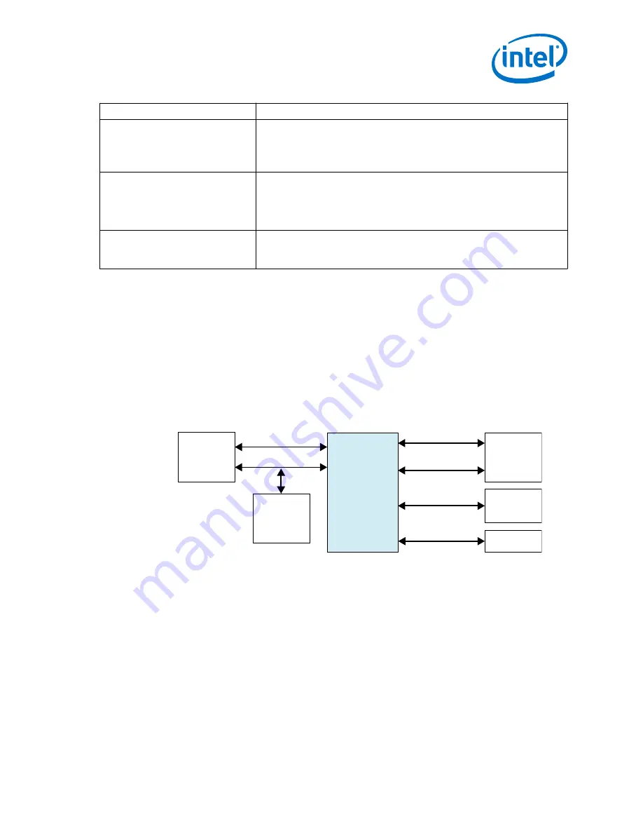
The JTAG topology of the board is shown in the figure below. An on-board USB Blaster
is implemented with the Intel MAX 10. It is in the form of a micro-USB type-B
connector (J9).
Figure 3.
JTAG topology block diagram
System
Intel
MAX 10
FPGA
USB PHY
CY7C68013
HDR2X5
for System Intel
MAX 10 FPGA
FMC
Configuration
Intel MAX 10
FX2 Bus 3.3 V
PD[3:0] (JTAG)
3.3 V
Intel
Cyclone 10
FPGA
JTAG 1.8 V
USB Configuration
1.8 V
JTAG 3.3 V
JTAG 3.3 V
The system Intel MAX 10 device itself can be configured through on-board USB port or
an external USB-Blaster II header. the 2x5 header for Intel MAX 10 is not mounted by
default.
A secondary Intel MAX 10 device is used for PFL configuration mode. This CFG Intel
MAX 10 is configured with on-board USB port.
The Intel Cyclone 10 GX FPGA device is configured with on-board USB port or an
external USB-Blaster II header.
The FMC interface also has a JTAG interface. The FMC JTAG can also be included into
the JTAG chain.
The Intel Cyclone 10 GX device JTAG and FMC JTAG can be put included or isolated
from the JTAG chain by setting a DIP switch S5.
4 Development Board Components
UG-20105 | 2017.12.18
Intel
®
Cyclone
®
10 GX FPGA Development Kit User Guide
21


