


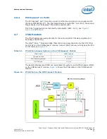


Intel
®
Atom™ Processor E660 with Intel
®
Platform Controller Hub EG20T Development Kit
January 2012
User Manual
Document Number: 324213-002
43
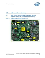
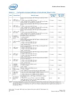
Reference Board Summary
Notes:
1.
When a switch is designated as 1–2, the switch slide is positioned such that pins 1 and 2 are shorted
together.
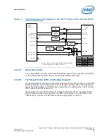
4.3.2
BSEL Jumper Settings
are provided to accommodate frequency selection for
the processor. The custom CK-505 clock chip (ICS9LPRS436BGLFT*) receives BSEL
signals from the Intel
®
Atom™ Processor E660 for frequency selection.
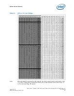
J60
COMe ATXPOW
UP control
select
PWROK signal to COMe Module select
1-2 short: Internal signal by D33VS and SUS_S3#
2-3 short: external signal by ATX-POW
1-2 short
1-2 short
J61
LVDS power
select
Onboard 5V or 12V supply select for LVDS backlight power
1-2 short: 5V supply at X53
2-3 short: 12V supply at X53
2-3 short
2-3 short
J62
Power SW to
COMe Select
Power SW signal to COMe module select
1-2 short: SW5 signal connect to COMe module directly
2-3 short: SW5 and Intel
®
PCH EG20T wake_out_n signal
merged signal connect to COMe module via CPLD
If the case to use the Wake On LAN in S5 state, it needs to set
2-3 short
2-3 short
2-3 short
Table 14.
Configuration Switch Settings on Carrier Board
Label
Switch
Name
Setting Context
Initial Setting
(AC Adapter Use
Case)
Initial Setting
(ATX-Power Use
Case)
SW1
RS-232C/485
select1
DB9 port (X19) is selected between RS232C and RS485.
1-2, 4-5, 7-8, 10-11 short: RS232C
2-3, 5-6, 8-9, 11-12 short: RS485
1-2, 4-5, 7-8, 10-11 short
(for RS232C setting)
1-2, 4-5, 7-8, 10-11 short
(for RS232C setting)
SW2
RS-232C/485
select2
DB9 port (X19) is selected between RS232C and RS485.
1-2, 4-5, 7-8, 10-11 short: RS232C
2-3, 5-6, 8-9, 11-12 short: RS485
1-2, 4-5, 7-8, 10-11 short
(for RS232C setting)
1-2, 4-5, 7-8, 10-11 short
(for RS232C setting)
SW3
RS-232C/485
select3
DB9 port (X19) is selected between RS232C and RS485.
1-2 short: RS232C
2-3 short: RS485
1-2 short
(for RS232C setting)
1-2 short
(for RS232C setting)
SW4
bit1: PCIe-
signal select dip
switch
bit 1: PCIe* Lane 3 connection on signal switch (U3) select
ON: PCI Express* Slot (X10) connection
OFF: PCI Express* Mini Card (X8) connection
bit 1: ON
(for PCI Express* Slot X10)
bit 1: ON
(for PCI Express Slot* X10)
bit3-8: Not used
bit3-5: No assign on the board
bit6-8: it is connected to CPLD, but it is not used
bit 3-8: OFF
bit 3-8: OFF
SW5
POWER push
switch
Non Lock push button (Push to ON)
ON: PWRBTN# to COMe Module is asserted.
OFF: PWRBTN# to COMe Module is de-asserted.
OFF
OFF
SW6
RESET push
switch
Non Lock push button (Push to ON)
ON: FPRST# to SIO is asserted.
OFF: FPRST# to SIO is de-asserted.
OFF
OFF
Table 13.
Configuration Jumper Settings on Carrier Board (Sheet 3 of 3)
Label
Jumper Name
Setting Context
Initial Setting
(AC Adapter
Use Case)
Initial Setting
(ATX-Power
Use Case)
Note:
A jumper consists of two or more pins mounted on the board. When a jumper cap is placed over two pins, it is
designated as SHORT. When there are more than two pins on the jumper, the pins to be shorted are indicated as 1–2 (to
short pin 1 to pin 2), 2–3 (to short pin 2 to pin 3), etc. When no jumper cap is to be placed on the jumper, it is
designated as OPEN.