background image

Chapter 2  Installations 

CI7BM User’s Manual 

15 


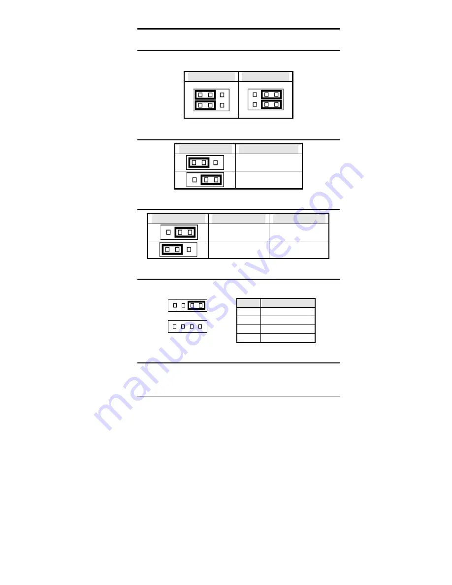
JP1: LCD Power Setting 


The CI7BM XGA interface supports 5V and 3.3V LCD displays. Use 
JP1 to change between 5V (

default

) and 3.3V panel video signal level. 


3.3V Setting 

5V Setting 

2     4     6 


1     3     5


2     4     6


1     3     5


JP4: DiskOnChip BIOS Expansion Address Select 


JP4 

Address 


 1


3


D0000-D7FFF 


1

 3


D8000-DFFFF (default) 


JP5: Clear CMOS Content 


JP5 

Setting 

Function 


 1

3


Pin 2-3 

Short/Closed


Clear CMOS Content 


1

3


Pin 1-2 

Short/Closed


Normal Operation 


JP7: External Battery Connector 

JP7connects to an external battery to maintain the information stored in 
the CMOS RAM in case the built-in battery malfunctions. 

Pin # 

Signal Name 

Vcc  

2  

N.C. 

3 Battery 

GND 

4 Ground 

1


4


Internal Battery (default) 

1


4


External Battery


JP8: On Board VGA Enable/Disable 


The on board VGA jumper, by default, is set to 

VGA Enable

 (pin 1-2 

short). To disable the VGA, short pin 2-3. 


Summary of Contents for CI7BM

Page 1: ...CI7BM Series Full Size Socket 370 All in one CPU Card Version 1 0D Industrial CPU Card PC Based Computer Boards for Industrial Automation User s Manual ...

Page 2: ...r be liable for direct indirect special exemplary incidental incidental or consequential damages resulting from any defect or omission in this manual even if advised of possibility of such damages The material contained herein is for informational purposes only Acknowledgments Award is a registered trademark of Award Software International Inc IBM and PS 2 are trademarks of International Business ...

Page 3: ... 768MB 768MB 768MB Memory Sockets 3 x DIMM 3 x DIMM 3 x DIMM VGA CRT LCD C T 69000 C T 69000 C T 69000 Watchdog Timer 16 level 16 level 16 level PC 104 Connector yes Yes yes Multi I O Chip Winbond 83977 Winbond 83977 Winbond 83977 Enhanced IDE yes yes yes 2S 1P yes yes yes USB yes yes yes IrDA yes yes yes Ultra2 SCSI no AIC 7890 no Audio on board CT2511 CT2511 no Ethernet 10 100Mbps Intel 82558B I...

Page 4: ...2 Connectors on the CI7BM 17 Watchdog Timer Configuration 36 Chapter 3 BIOS Configuration 38 Chapter 4 Intel PIIX Bus Master IDE Driver Installation 64 Chapter 5 VGA Driver Installation 68 Chapter 6 Audio Driver Installation 71 Chapter 7 LAN Driver Installation Guide 74 Chapter 8 System Monitor Utility 80 Chapter 9 LANDesk Client Manager 88 Chapter 10 SCSI Installation Guide 96 Appendix 107 A I O ...

Page 5: ...nformation on the CI7BM CPU card It is divided into the following sections Checklist 2 Description 2 Features 3 Specifications 3 Intelligence 5 Board Dimensions 7 The topics covered in this chapter are as follows Checklist Description Features Specifications Layout of Key Components and Dimensions ...

Page 6: ...tility 1 Optional CD containing Intel LANDesk Client Manger 4 Diskettes Containing Adaptec Ultra2 SCSI Driver applies for CI7BM 8 Diskettes Containing Creative Labs CT2511 Driver applies for CI7BM CI7BM and CI7BMV Description The CI7BM is an Industrial CPU card based on the Intel 440BX chipset and is fully designed for harsh industrial environment It features a Socket 370 processor connector that ...

Page 7: ...CP EPP parallel port PC 104 extension Hardware Monitoring Windows shut off Modem ring on 10 100M Base T Ethernet interface Novell NE2000 Compatible Specifications Processor Socket Socket 370 connector Processor Intel Celeron 66MHz FSB Coppermine 100MHz FSB is supported on CI7BM with PCB version 1 10 or above Chipset Intel 440BX AGPset with PCI EIDE and RTC built in Secondary Cache CPU integrated M...

Page 8: ... or Ultra DMA 33 IDE Hard Disk and ATAPI CD ROM FDD Interface Two floppy drives 360KB 720KB 1 2MB 1 44MB 2 88MB LS 120 CRT LCD C T 69000 chipset Embedded 2MB SDRAM display memory Simultaneous CRT LCD display LCD panel supports DSTN TFT 1280x1024x8bpp colors CRT resolution Up to 1280x1024x8bpp colors resolution for color active matrix TFT panels 12 18 and 24bit analog or 12 12 18 18 double pixel CL...

Page 9: ...r IrDA Interface Pin header connector for the optional IrDA external connector PICMG Compliance Fully compliant to PICMG standards Environmental and Mechanical Power Supply 10A 5V max 12V 100mA max Temperature 0 C to 60 C Humidity 5 to 95 Dimensions 338mm x 122mm Intelligence Temperature Monitoring and Alert A sensor for the CPU temperature on the CI7BM monitors the CPU temperature and alerts the ...

Page 10: ...Chapter 1 Introduction 6 CI7BM User s Manual Wake On LAN Through an ATX power supply and network connection systems can be turned on from the power off state ...

Page 11: ...Chapter 1 Introduction CI7BM User s Manual 7 Board Dimensions ...

Page 12: ... chapter provides information on how to use the jumpers and connectors on the CI7BM in order to set up a workable system The topics covered are CPU Installation 9 Memory Installation 10 Jumpers on the CI7BM 12 Connectors on the CI7BM 17 Watchdog Timer Configuration 36 ...

Page 13: ...erting the CPU make sure the lever is raised perpendicular to the socket and the notch on the corner of the CPU corresponds with the notch on the inside of the socket After you have installed and lock the processor into place check if the jumpers for the CPU type and speed are correct NOTE Ensure that the CPU heat sink and the CPU top surface are in total contact to avoid CPU overheating problem t...

Page 14: ...ble on how to configure the memory NOTE Use SDRAM modules with PC100 specification when running 100MHz CPU bus speed With 66MHz CPU bus speed SDRAM modules with PC66 or PC100 specification can be used You have to install the Pentium II processor before installing the memory modules 168 pin DIMM 3 3V Unbuffer SDRAM Bank0 DIMM3 Bank1 DIMM2 Bank2 DIMM1 Total Memory 8MB 8MB 16MB 16MB 32MB 32MB 64MB 64...

Page 15: ...B 8MB 72MB 64MB 32MB 8MB 104MB 128MB 32MB 8MB 168MB 32MB 32MB 16MB 80MB 64MB 32MB 16MB 112MB 128MB 32MB 16MB 176MB 32MB 32MB 32MB 96MB 64MB 32MB 32MB 128MB 128MB 32MB 32MB 192MB 64MB 64MB 128MB 128MB 64MB 192MB 64MB 64MB 8MB 136MB 128MB 64MB 8MB 200MB 64MB 64MB 16MB 144MB 128MB 64MB 16MB 208MB 64MB 64MB 32MB 160MB 128MB 64MB 32MB 224MB 64MB 64MB 64MB 192MB 128MB 64MB 64MB 256MB 128MB 128MB 320MB 1...

Page 16: ...ve The following table lists the connectors on CI7BM and their respective functions Jumper Locations on the CI7BM 13 DSW1 3 CPU Bus Speed Selector 13 DSW1 5 8 CPU Frequency Selector 13 JP1 LCD Power Setting 14 JP4 DiskOnChip BIOS Expansion Address Select 15 JP5 Clear CMOS Content 15 JP7 External Battery Connector 15 JP8 On Board VGA Enable Disable 14 JP9 RS232 422 485 COM2 Selection 16 JP12 On Boa...

Page 17: ...Chapter 2 Installations CI7BM User s Manual 13 Jumper Locations on the CI7BM ...

Page 18: ...off on 5X 333MHz 500MHz xx xx xx xx off on on on 5 5X 366MHz 550MHz xx xx xx xx off off off on 6X 400MHz 600MHz xx xx xx xx on on on off 6 5X 433MHz 650MHz xx xx xx xx on on off off 7X 466MHz 700MHz xx xx xx xx on off off on 7 5X 500MHz 750MHz xx xx xx xx on off off off 8X 533MHz 800MHz xx xx xx xx off on on off Note The settings for 650MHz 700MHz 750MHz and 800MHz frequencies are for reference on...

Page 19: ...F default JP5 Clear CMOS Content JP5 Setting Function 1 3 Pin 2 3 Short Closed Clear CMOS Content 1 3 Pin 1 2 Short Closed Normal Operation JP7 External Battery Connector JP7connects to an external battery to maintain the information stored in the CMOS RAM in case the built in battery malfunctions Pin Signal Name 1 Vcc 2 N C 3 Battery GND 4 Ground 1 4 Internal Battery default 1 4 External Battery ...

Page 20: ...RS 485 Jumper Setting pin closed all jumpers open 1 2 3 4 5 6 7 8 11 12 15 16 17 18 19 20 23 24 1 2 3 4 5 6 7 8 9 10 11 12 13 14 15 16 17 18 19 20 21 22 1 2 1 2 1 2 3 4 3 4 3 4 5 6 5 6 5 6 7 8 7 8 7 8 9 10 9 10 9 10 11 12 11 12 11 12 13 14 13 14 13 14 15 16 15 16 15 16 17 18 17 18 17 18 19 20 19 20 19 20 21 22 21 22 21 22 23 24 23 24 23 24 Jumper Illustration JP9 JP9 JP9 JP12 On Board LAN Enable D...

Page 21: ... LAN Connector 23 J5 Floppy Drive Connector 24 JP6 SB Link Connector 24 J6 Flat Panel LCD Connector 25 Flat Panel Display Interface Pin Descriptions 25 J7 Parallel Port Connector 27 J8 COM1 Serial Port 28 J9 COM2 Serial Port 28 J10 External SCSI HDD LED 29 J11 Audio I O Connector 29 J12 Ultra2 SCSI Connector 30 J14 Chassis Fan Power Connector 31 J15 External ATX Power Connector 31 J17 PS 2 Keyboar...

Page 22: ...Chapter 2 Installations 18 CI7BM User s Manual Connector Locations on the CI7BM ...

Page 23: ...Reset Switch Turbo LED Connector ATX Power On Switch SMI Hardware Switch Power LED and Keylock Speaker Speaker Pins 1 4 This connector provides an interface to a speaker for audio tone generation An 8 ohm speaker is recommended Pin Signal Name 1 Speaker out 2 No connect 3 Ground 4 5V Power LED and Keylock Pins 11 15 The power LED indicates the status of the main power switch The keylock switch whe...

Page 24: ...connects to the power switch on the case When pressed the power switch will force the system to power on When pressed again it will force the system to power off Turbo LED Connector Pins 8 and 18 There is no turbo deturbo function on the CPU card The Turbo LED on the control panel will always be On when attached to this connector Pin Signal Name 8 5V 18 Ground Reset Switch Pins 9 and 19 The reset ...

Page 25: ...nel This LED will flash when the HDD is being accessed Pin Signal Name 10 Ground 20 5V J2 External Keyboard Connector 1 Pin Signal Name 1 Keyboard clock 2 Keyboard data 3 NC 4 GND 5 5 Vcc J2 JP2 IrDA Connector This connector is used for an IrDA connector for wireless communication Pin Signal Name 1 5V 2 No connect 3 Ir TX 4 Ground 5V IRTX IRRX N C GND 5 Ir RX ...

Page 26: ...ost data 10 Host data 4 9 10 Host data 11 Host data 3 11 12 Host data 12 Host data 2 13 14 Host data 13 Host data 1 15 16 Host data 14 Host data 0 17 18 Host data 15 Ground 19 20 Key DRQ0 21 22 Ground Host IOW 23 24 Ground Host IOR 25 26 Ground IOCHRDY 27 28 Host ALE DACK0 29 30 Ground IRQ14 31 32 No connect Address 1 33 34 No connect Address 0 35 36 Address 2 Chip select 0 37 38 Chip select 1 J3 ...

Page 27: ...a 15 Ground 19 20 Key DRQ1 21 22 Ground Host IOW 23 24 Ground Host IOR 25 26 Ground IOCHRDY 27 28 Host ALE DACK1 29 30 Ground IRQ15 31 32 No connect Address 1 33 34 No connect Address 0 35 36 Address 2 Chip select 0 37 38 Chip select 1 J4 Activity 39 40 Ground JP3 Wake On LAN Connector JP3 is a 3 pin header for the Wake On LAN function on the CPU card The following table shows the pin out assignme...

Page 28: ...ound 19 20 Step Ground 21 22 Write data Ground 23 24 Write gate Ground 25 26 Track 00 Ground 27 28 Write protect Ground 29 30 Read data Ground 31 32 Side 1 select J5 Ground 33 34 Diskette change JP6 SB Link Connector The following table shows the pin out assignments of this connector This connector is used for the Creative Sound AWE64D PCI sound card The SB Link uses Intel s PC PCI technology to d...

Page 29: ...ND 3 4 GND 5V 3 3V 5 6 5V 3 3V ENPVEE 7 8 GND PD0 9 10 PD1 58 57 PD2 11 12 PD3 PD4 13 14 PD5 PD6 15 16 PD7 PD8 17 18 PD9 PD10 19 20 PD11 PD12 21 22 PD13 PD14 23 24 PD15 PD16 25 26 PD17 PD18 27 28 PD19 PD20 29 30 PD21 PD22 31 32 PD23 GND 33 34 GND SHFCLK 35 36 FLM M 37 38 LP 2 1 GND 39 40 ENABKL GND 41 42 ASCLK ENAVDD 43 44 5V 3 3V NC 45 46 NC J6 PD24 47 48 PD25 PD26 49 50 PD27 PD28 51 52 PD29 PD30...

Page 30: ...2 UD2 G0 B5 FB5 SB1 R5 B2 LG1 LG0 LB0 P6 D6 LD1 UD1 G1 B6 SB0 SB2 B5 R3 LB1 LB0 UR1 P7 D7 LD0 UD0 G2 B7 SB1 B3 G3 LR2 LR1 UG1 P8 LD7 G3 G0 SB2 FG0 B3 UG1 UB1 P9 LD6 G4 G1 SB3 FG1 R4 UB1 LR1 P10 LD5 G5 G2 SB4 FG2 G4 UR2 LG1 P11 LD4 R0 G3 SB5 FG3 B4 UG2 LB1 P12 LD3 R1 G4 FG0 SG0 R5 LG1 UR2 P13 LD2 R2 G5 FG1 SG1 G5 LB1 UG2 P14 LD1 R3 G6 FG2 SG2 B5 LR2 UB2 P15 LD0 R4 G7 FG3 SG3 G6 LG2 LR2 P16 R0 FG4 F...

Page 31: ...e printer strobe 1 14 AutoFeed PD0 parallel data 0 2 15 Error PD1 parallel data 1 3 16 Initialize PD2 parallel data 2 4 17 Select PD3 parallel data 3 5 18 Ground PD4 parallel data 4 6 19 Ground PD5 parallel data 5 7 20 Ground PD6 parallel data 6 8 21 Ground PD7 parallel data 7 9 22 Ground ACK acknowledge 10 23 Ground Busy 11 24 Ground Paper empty 12 25 Ground J7 Select 13 N A N A ...

Page 32: ...XD Transmit data 4 DTR Data terminal ready 5 GND ground 6 DSR Data set ready 7 RTS Request to send 8 CTS Clear to send J8 COM1 9 RI Ring indicator 10 NC J9 COM2 Serial Port J9 a 10 pin header connector is the onboard COM2 serial port of the CI7BM The following table shows its pin assignments Pin Signal Name RS 232 R2 422 RS 485 1 DCD TX DATA 2 RX TX DATA 3 TX RX NC 4 DTR RX NC 5 GND GND GND 6 DSR ...

Page 33: ...R Out L 5 6 GND Auxi L 7 8 Auxi R GND 9 20 Line R Line L 11 12 GND NC 13 14 NC Vcc 15 16 MIC RxD 17 18 TXD GP7 19 20 GP6 GP5 21 22 GP4 GP3 23 24 GP2 J11 GP1 25 26 GP0 The J11 Audio I O Connector connects to the EXTVGM Audio Daughter Card with the 26 pin ribbon cable supplied with the package The EXTVGM Audio Daughter card provides two CD AUDIO IN internal connectors and external connectors for LIN...

Page 34: ...LVDM2 LVDP3 9 43 LVDM3 LVDP4 10 44 LVDM4 LVDP5 11 45 LVDM5 LVDP6 12 46 LVDM6 LVDP7 13 47 LVDM7 LVDPLP 14 48 LVDPLM GROUND 15 49 GROUND DFFSENSE 16 50 LVEXT68 GROUND 17 51 LVTRMPWR LVTRMPWR 18 52 LVTRMPWR LVTRMPWR 19 53 N C GROUND 20 54 GROUND LVATNP 21 55 LVATNM GROUND 22 56 GROUND LVBSYP 23 57 LVBSYM LVACKP 24 58 LVACKM LVRSTP 25 59 LVRSTM LVMSGP 26 60 LVMSGM LVSELP 27 61 LVSELM LVCDP 28 62 LVCDM...

Page 35: ... chassis fan The fan must be a 12V fan Pin Signal Name 1 Rotation 2 12V 1 2 3 3 Ground J15 External ATX Power Connector Pin Signal Name 1 N C 2 GND 3 N C 4 GND 5 PS ON soft on off 1 6 6 5V SB standby 5V J15 J17 PS 2 Keyboard Connector Pin Signal Name 1 Keyboard data 2 N C 3 GND 4 5V 5 Keyboard clock J17 6 N C ...

Page 36: ...A CRT connector are as follows Signal Name Pin Pin Signal Name Red 1 2 Green Blue 3 4 N C GND 5 6 GND GND 7 8 GND N C 9 10 GND N C 11 12 N C HSYNC 13 14 VSYNC J19 NC 15 J20 RJ45 Connector This connector is for the 10 100Mbps Ethernet capability of the CPU card The figure below shows the pin out assignments of this connector and its corresponding input jack J20 TD pin 1 TD pin 2 RD pin 3 RD pin 6 ...

Page 37: ...s a 3 pin header for the CPU fan The fan must be a 12V fan Pin Signal Name 1 Rotation 2 12V 1 2 3 3 Ground J23 J24 USB Connectors The following table shows the pin outs of the USB connectors J24 Pin J23 Pin Signal Name 1 1 Vcc 2 2 USB 3 3 USB J24 1 2 3 4 USB J23 1 2 3 4 4 4 Ground ...

Page 38: ...A7 D2 B7 12V C7 LA19 D7 IRQ15 A8 D1 B8 OWS C8 LA18 D8 IRQ14 A9 D0 B9 12V C9 LA17 D9 DACK0 A10 IOCHRDY B10 GND C10 MEMR D10 DRQ0 A11 AEN B11 SMEMW C11 MEMW D11 DACK5 A12 A19 B12 SMEMR C12 D8 D12 DRQ5 A13 A18 B13 IOW C13 D9 D13 DACK6 A14 A17 B14 IOR C14 D10 D14 DRQ6 ZA15 A16 B15 DACK3 C15 D11 D15 DACK7 A16 A15 B16 DRQ3 C16 D12 D16 DRQ7 A17 A14 B17 DACK1 C17 D13 D17 VCC A18 A13 B18 DRQ1 C18 D14 D18 M...

Page 39: ... LED3 LAN Activity Indicators LED2and LED3 are orange and yellow LED indicators located at the bracket side of the CPU card that shows LAN activity and the transfer rate in progress Refer to the following table for the functions of each LED status LED2 yellow Status Function LED3 green Status Function ON Data transfer in progress OFF 10Mbps transfer rate OFF Data transfer off Link off ON 100Mbps t...

Page 40: ...t 0441H for the system to stop the watchdog function The timer has a tolerance of 20 for its intervals The following describes how the timer should be programmed Enabling Watchdog MOV AX 000FH Choose the values from 0 MOV DX 0443H OUT DX AX Disabling Watchdog MOV AX 00FH Any value is fine MOV DX 0441H OUT DX AX WATCHDOG TIMER CONTROL TABLE Level Value Time sec Level Value Time sec 1 F 0 9 7 16 2 E...

Page 41: ...Chapter 2 Installations CI7BM User s Manual 37 This page was intentionally left blank ...

Page 42: ...r describes the different settings available in the Award BIOS The topics covered in this chapter are as follows BIOS Introduction 41 BIOS Setup 41 Standard CMOS Setup 43 Date 43 Time 44 Primary HDDs Secondary HDDs 44 Drive A Drive B 45 Video 45 Halt On 45 BIOS Features Setup 46 Virus Warning 46 CPU Internal Cache External Cache 46 CPU L2 Cache ECC Checking 47 Quick Power On Self Test 47 Boot Sequ...

Page 43: ...M CAS Latency Time 49 Bank DRAM Timing 49 DRAM Clock 50 SDRAM Precharge Control 50 SDRAM Cycle Length 50 Memory Hole 50 Read Around Write 50 Concurrent PCI Host 50 Video RAM Cacheable 50 DRAM Data Integrity Mode 50 System BIOS Cacheable 50 Video BIOS Cacheable 51 Video RAM Cacheable 51 8 Bit I O Recovery Time 51 16 Bit I O Recovery Time 51 Memory Hole at 15MB 16MB 51 Passive Release 51 Delayed Tra...

Page 44: ...lled 56 Resources Controlled by 56 Reset Configuration Data 56 IRQ3 4 5 7 9 10 11 12 14 15 DMA0 1 3 5 6 7 assigned to 56 Load BIOS Defaults 57 Load Setup Defaults 57 Integrated Peripherals 58 IDE HDD Block Mode 58 IDE Primary Secondary Master Slave PIO 58 IDE Primary Secondary Master Slave UDMA 58 On Chip Primary Secondary PCI IDE 59 Onboard PCI SCSI Chip 59 USB Keyboard Support 59 Init AGP Displa...

Page 45: ... the Award BIOS is immediately activated Pressing the Del key immediately allows you to enter the Setup utility If you are a little bit late pressing the Del key POST Power On Self Test will continue with its test routines thus preventing you from invoking the Setup If you still wish to enter Setup restart the system by pressing the Reset button or simultaneously pressing the Ctrl Alt and Delete k...

Page 46: ...Hard Disk Type The section below the setup items of the Main Menu displays the control keys for this menu Another section at the bottom of the Main Menu just below the control keys section displays information on the currently highlighted item in the list NOTE After making and saving system changes with Setup you find that your computer cannot boot the Award BIOS supports an override to the CMOS s...

Page 47: ...Auto 0 0 0 0 0 0 Auto Primary Slave Auto 0 0 0 0 0 0 Auto Secondary Master Auto 0 0 0 0 0 0 Auto Secondary Slave Auto 0 0 0 0 0 0 Auto Drive A 1 44M 3 5in Base Memory 640K Drive B None Extended Memory 15360K Other Memory 384K Video EGA VGA Halt On All Errors Total Memory 16384K ESC Quit Ç È Æ Å Select Item PU PD Modify F1 Help Shift F2 Change Color At the bottom of the menu are the control keys fo...

Page 48: ...able For the Primary Master Slave as well as Secondary Master Slave you can select Auto under the TYPE and MODE fields This will enable auto detection of your IDE drives and CD ROM drive during POST Press PgUp PgDn to select a numbered hard disk type or type the number and press the Enter key The hard disk will not work properly if you enter incorrect information for this field If your hard disk d...

Page 49: ...ur system You can choose the following video display cards EGA VGA For EGA VGA SEGA SVGA or PGA monitor adapters default CGA 40 Power up in 40 column mode CGA 80 Power up in 80 column mode MONO For Hercules or MDA adapters Halt On This field determines whether the system will halt if an error is detected during power up No errors The system boot will not be halted for any error that may be detecte...

Page 50: ...rt No FDD For WIN 95 Yes F1 Help PU PD Modify F5 Old Values Shift F2 Color F6 Load BIOS Defaults F7 Load Setup Defaults Virus Warning This item protects the boot sector and partition table of your hard disk against accidental modifications If an attempt is made the BIOS will halt the system and display a warning message If this occurs you can either allow the operation to continue or run an anti v...

Page 51: ... so that Drive A becomes Drive B and Drive B becomes Drive A By default this field is set to Disabled Boot Up Floppy Seek When enabled the BIOS will seek whether or not the floppy drive installed has 40 or 80 tracks 360K type has 40 tracks while 760K 1 2M and 1 44M all have 80 tracks By default this field is set to Enabled Boot Up NumLock Status This allows you to activate the NumLock function aft...

Page 52: ...standard VGA display cards may not show colors properly This field allows you to set whether MPEG ISA VESA VGA Cards can work with PCI VGA or not When this field is enabled a PCI VGA can work with a MPEG ISA VESA VGA card When this field is disabled a PCI VGA cannot work with a MPEG ISA VESA Card OS Select for DRAM 64MB This option allows the system to access greater than 64MB of DRAM memory when ...

Page 53: ... Transaction Disabled ESC Quit Ç È Æ Å Select Item F1 Help PU PD Modify F5 Old Values Shift F2 Color F6 Load BIOS Defaults F7 Load Setup Defaults SDRAM RAS to CAS Delay When DRAM is refreshed both rows and columns are addressed separately This field allows you to determine the timing of transition from Row Address Stove RAS to Column Address Strobe CAS SDRAM RAS Precharge Time The precharge time i...

Page 54: ...led Read Around Write DRAM optimization feature If a memory read is addressed to a location whose latest write is being held in a buffer before being written to memory the read is satisfied through the buffer contents and the read is not sent to the DRAM The default setting is Enabled Concurrent PCI Host This field enables or disables the concurrent PCI Host The default setting is Disabled Video R...

Page 55: ... default setting is 2 Memory Hole at 15MB 16MB In order to improve performance certain space in memory can be reserved for ISA cards This field allows you to reserve 15MB to 16MB memory address space to ISA expansion cards This makes memory from 15MB and up unavailable to the system Expansion cards can only access memory up to 16MB By default this field is set to Disabled Passive Release When enab...

Page 56: ... These read only fields show the current speeds in RPM revolution per minute for the CPU fan and chassis fan as monitored by the hardware monitoring IC VCCP VTT VCC3 These read only fields show the current voltages in the voltage regulators and power supply as monitored by the hardware monitoring IC Shutdown Temperature This field allows you to set the temperature at which the system automatically...

Page 57: ... PWR BTTN Instant Off PowerOn by Ring Disabled Resume by Alarm Disabled ESC Quit Ç È Æ Å Select Item IRQ 8 Break Suspend Disabled F1 Help PU PD Modify F5 Old Values Shift F2 Color F6 Load BIOS Defaults F7 Load Setup Defaults ACPI function ACPI stands for Advanced Configuration Power Interface The default setting of this field Enabled Power Management This field allows you to select the type of pow...

Page 58: ...interrupt request IRQ line assigned to the modem if any on your system Activity of the selected IRQ always awakens the system By default the IRQ is set to 3 Doze Mode When enabled and after the set time of system inactivity the CPU clock will run at a slower speed while all other devices still operate at full speed Standby Mode After the selected period of system inactivity the fixed disk drive an...

Page 59: ...itoring of IRQ 8 Real Time Clock so it does not awaken the system from Suspend mode Reload Global Timer Events This section determines the reloading of the timers after entering the Full On You can enable or disable the monitoring of IRQ 8 Real Time Clock so it does not awaken the system from Suspend mode PM Events The VGA LPT COM HDD FDD DMA master PWR On by Modem LAN RTC Alarm Resume and Primary...

Page 60: ...dify DMA 5 assigned to PCI ISA PnP F5 Old Values Shift F2 Color DMA 6 assigned to PCI ISA PnP F6 Load BIOS Defaults DMA 7 assigned to PCI ISA PnP F7 Load Setup Defaults PNP OS Installed This field allows you to specify if the operating system installed in your system is plug and play aware NOTE Operating systems such as DOS OS 2 and Windows 3 x do not use PnP Resources Controlled by This PnP BIOS ...

Page 61: ...lor Load BIOS Defaults except Standard CMOS Setup To load BIOS defaults value to CMOS SRAM enter Y If not enter N Load Setup Defaults This option allows you to load the default values to your system configuration These default settings are optimal and enable all high performance features ROM PCI ISA BIOS CMOS SETUP UTILITY AWARD SOFTWARE INC STANDARD CMOS SETUP CPU SPEED SETTING BIOS FEATURES SETU...

Page 62: ...ort 1 3F8 IRQ4 F1 Help PU PD Modify Onboard Serial Port 2 2F8 IRQ3 F5 Old Values Shift F2 Color UART Mode Select Normal F6 Load BIOS Defaults F7 Load Setup Defaults IDE HDD Block Mode This field allows your hard disk controller to use the fast block mode to transfer data to and from your hard disk drive IDE Primary Secondary Master Slave PIO These fields allow your system hard disk controller to w...

Page 63: ...FDC Controller Select Enabled if your system has a floppy disk controller FDC installed on the system and you wish to use it If you install an add in FDC or the system has no floppy drive select Disabled in this field This option allows you to select the onboard FDD port Onboard Serial Parallel Port These fields allow you to select the onboard serial and parallel ports and their addresses The defa...

Page 64: ...etting a password the screen automatically returns to the main screen To disable a password just press the Enter key when you are prompted to enter the password A message will confirm the password to be disabled Once the password is disabled the system will boot and you can enter Setup freely ROM PCI ISA BIOS CMOS SETUP UTILITY AWARD SOFTWARE INC STANDARD CMOS SETUP CPU SPEED SETTING BIOS FEATURES...

Page 65: ...DZ SECTOR MODE Primary Master Select Primary Master Option N SKIP N OPTIONS TYPE SIZE CYLS HEAD PRECOMP LANDZ SECTOR MODE 1 Y 0 0 0 0 0 0 0 NORMAL NOTE Some OSes like SCO UNIX must use NORMAL for installation Up to four IDE drives can be detected with parameters for each appearing in sequence inside a box To accept the displayed entries press the Y key to skip to the next drive press the N key If ...

Page 66: ...SC Quit Ç È Æ Å Select Item F10 Save Exit Setup Shift F2 Change Color Save Data to CMOS Exit Setup Exit Without Saving Select this option to exit the Setup utility without saving the changes you have made in this session Typing Y will quit the Setup utility without saving the modifications Typing N will return you to Setup utility ROM PCI ISA BIOS CMOS SETUP UTILITY AWARD SOFTWARE INC STANDARD CMO...

Page 67: ...Chapter 3 BIOS Configuration CI7BM User s Manual 63 This page was intentionally left blank ...

Page 68: ...7BM User s Manual 4 Intel PIIX Bus Master IDE Driver Installation This chapter describes the installation procedure for Intel PIIX Bus Master IDE Drivers for Windows 95 This chapter contains the following sections System Requirements 65 Installing the Software 66 ...

Page 69: ...d to the system 3 One of the following versions of Windows 95 must be installed on the system prior to running utility program Windows 95 4 00 950 Retail Windows 95 4 00 950a OSR1 Windows 95 4 00 950b OSR2 without USB Supplement Windows 95 4 00 950b OSR2 1 with USB Supplement 4 This utility should only be used on desktop systems The utility must not be executed on notebook or portable systems with...

Page 70: ...gram that allows the driver files to be INSTALLED or DE INSTALLED Execute the driver setup program Run SETUP EXE 4 Click Next on Welcome Screen to read and agree to the license agreement View the text file and choose File Exit to close Notepad and continue NOTE If you click No program will terminate 5 Click Yes if you agree to continue NOTE If you click No the program will terminate 6 Select INSTA...

Page 71: ... scrollbar and click on the Windows 95 directory System IOSubSys path For example Click on C WINDOWS SYSTEM IOSUBSYS Click OK 9 Select Yes when prompted to re start Windows 95 NOTE After installation the following driver and related files are stored as listed Windows 95 directory System IOSubSys IDEATAPI MPD Windows 95 directory System IOSubSys PIIXVSD VXD Windows 95 directory INF IDEATAPI INF ...

Page 72: ...tions set forth in this chapter carefully Please note that there must be relevant software installed in your system before you could proceed to install the VGA drivers It is recommended that you make a copy of the VGA driver diskette and put the backup copy in a safe place The following items are covered in this chapter Installing the Drivers for Windows 95 69 Installing the Drivers for Windows 98...

Page 73: ...el icon 2 Double click Display 3 Click Settings 4 Click Advanced Properties 5 Click Change 6 Click Have Disk 7 Insert the diskette CD containing the 69000 VGA driver for Windows 95 to the floppy disk drive CD ROM drive then type in A WIN95 assuming drive A is your floppy disk drive or type in D VGA C T WIN95 assuming drive D is your CD ROM drive and press Enter 8 Select Chips and Tech 69000 PCI AG...

Page 74: ...lick Change 7 Click Next 8 Select Display a list of all the drivers in a specific location so you can select the driver you want 9 Click Have Disk 10 Insert the diskette CD containing the C T 69000 VGA driver for Windows 98 to the floppy disk drive CD ROM drive then type in A WIN98 assuming drive A is your floppy disk drive or type in D VGA C T WIN98 assuming drive D is your CD ROM drive and press...

Page 75: ...lick the Control Panel icon 4 Double click the Display icon 5 Click Change Display Type 6 Click Change 7 Click Have Disk then insert the diskette CD containing the C T 69000 VGA driver for Windows NT 4 0 to the floppy disk drive CD ROM drive then type in A WINNT40 assuming drive A is your floppy disk drive or type in D VGA C T WINNT40 assuming drive D is your CD ROM drive and press Enter 8 Select ...

Page 76: ...e Labs ViBRA 16VX that come in floppy diskettes with your package Please follow the instructions set forth in this chapter It is recommended that you make a copy of the audio driver diskette and put the backup copy in a safe place The following items are covered in this chapter Installing The Audio Driver For Windows 95 73 Installing The Audio Driver For Windows 98 73 ...

Page 77: ...etup wizard prompts you for the setup method it is recommended to choose FULL INSTALLATION Select this option and click Next Step 6 Upon completion of the software and driver installation the system will prompt you to restart the system Restart the system to activate the drivers Installing The Audio Driver For Windows 98 1 The Windows 98 operating system CD comes with the drivers for ViBRA 16VX In...

Page 78: ... LAN Driver Installation Guide This chapter describes LAN features and driver installation of the onboard Intel 82558B Ethernet controller The following items are covered in this chapter Introduction 74 Features 74 Software Drivers Support 74 Running Diagnostics 75 ...

Page 79: ...ernet IEEE 802 3u standard z Compatible with PCI Local Bus Revision 2 1 specification z IEEE 802 3u Auto Negotiation for automatic speed selection z Supports Full Duplex Half Duplex Operation z Provides 32 bit bus mastering data transfer z Supports 10Mbps and 100Mbps operation in a single port z Supports remote wake up Magic Packet in APM and ACPI mode Requires ATX power supply with 5VSB 720mA Sof...

Page 80: ...u Automatic setup View adapter configuration Test adapter Install network drivers View Help files Exit Setup Choose AUTOMATIC SETUP to view the adapter s configuration make sure it works properly and install the software needed to connect to your network Help F1 Exit Esc Select Action 2 Selecting View adapter configuration will show the following 8255x based PCI EtherExpress adapter Setup V4 16 Vi...

Page 81: ... Onboard loopback tests passed Network test passed 10Mbps This adapter works properly Press Enter to continue Help F1 Press Enter to continue 4 Selecting Install network drivers will show the following screen 8255x based PCI EtherExpress adapter Setup V4 16 Main Menu Install network drivers Novel Microsoft Other Exit Setup Choose OTHER if you use a network operating system from a manufacturer not ...

Page 82: ...driver information Choose OTHER if you use a network operating system from a manufacturer not on this list such as Banyan or UNIX Help F1 Previous Esc Select Accept 6 Selecting View Help files under the Main menu will show the following screen 8255x based PCI EtherExpress adapter Setup V4 16 Main Menu View Help files Installing EtherExpress PRO 100 adapter drivers Latest News and general adapter i...

Page 83: ...Chapter 7 LAN Driver Installation Guide CI7BM User s Manual 79 This page was intentionally left blank ...

Page 84: ...User s Manual 8 System Monitor Utility This chapter introduces System Monitor Utility that comes with the CPU card in conjunction with the onboard hardware monitoring IC The sections in the following pages describe the functions of the utility ...

Page 85: ...onditions become adverse that is when voltages are erratic or CPU temperature exceeds the safe limits an alarm will be sounded thereby preventing system crashing and ensuring overall stability NOTE System Monitor currently supports English and Chinese under Windows 95 and Windows NT English will be used for other language environments When System Monitor is initiated the icon below appears in the ...

Page 86: ...on the System Monitor icon Clicking on the upper left corner button would show you the latest company information Summary provides the current system status The section below describes the different functions of System Monitor 1 Computer displays the current working system version and processor type ...

Page 87: ...Chapter8 System Monitor Utility CI7BM User s Manual 83 2 Power displays the current voltage status ...

Page 88: ...Chapter 8 System Monitor Utility 84 CI7BM User s Manual 3 Memory displays the current memory usage status ...

Page 89: ...Chapter8 System Monitor Utility CI7BM User s Manual 85 4 Fan Speed displays the current rotational speeds of CPU and Chassis fans 5 Disk displays the supported disk formats and disk space ...

Page 90: ...Chapter 8 System Monitor Utility 86 CI7BM User s Manual 6 Heat displays the CPU and system temperatures 7 Error Log displays errors occurring after System Monitor is started ...

Page 91: ...ge the acceptable voltage range between the MAX and MIN value Temperature temperature threshold Fan Rotation Speed the minimum rotation speed NOTE Intel has defined a margin of difference for the voltages as below 12 Volts 10 10 8V 13 2V 5 Volts 5 4 75 5 25 Vio 5 Vio for P54C CPU is 3 5V Vio for P55C is 3 3V Vcore 5 ...

Page 92: ...pter gives a brief introduction to the optional LANDesk Client Manager LDCM utility as well as the installation procedures The following items are covered in this chapter Introduction 89 Installation 90 Installing the Local Version of LDCM 91 Installing the Administrative Version of LDCM 93 ...

Page 93: ...e ability to gather information about remote PCs as well as remotely controlling the PCs The remote access is based upon granted rights by the managed client LDCM provides the user with self help diagnostics including a PC health meter local alerting of potential problems and hardware and software inventory Automatic polling and alerting of memory and hardware conditions and predictive failure mec...

Page 94: ...system Upon entering the Windows NT 4 0 or Windows 95 environment insert the CD Windows will autorun the installation program and show the following screen NOTE During Setup you will be asked to install Internet Explorer 3 02 in order to continue or else Setup will be aborted LDCM supports various languages and will default to English if it is unable to load language dl ...

Page 95: ...talling the Local Version of LDCM Double Click on LANDesk Client Manager in the initial screen and the following screen will appear Double click on the local version of LANDesk Client Manager When the Welcome screen appears click on Next to continue with Setup ...

Page 96: ...on where Setup will install LANDesk Client Manager Click Browse if you want to change the directory suggested Otherwise click Next to start installing LDCM When Setup is finished changes will have been made to the file AUTOEXEC BAT Restart your computer for the changes to take effect ...

Page 97: ...ient Manager in the initial screen select the administrative version of the LDCM and the Welcome screen below will appear Click on Next to continue The screen below allows you to install the documentation in Adobe Acrobat format and the Adobe Acrobat Reader software Select the options you need and click on Next to start the installation ...

Page 98: ...Chapter 9 LANDesk Client Manager 94 CI7BM User s Manual After LANDesk Client Manager Setup is complete restart your computer to be able to use the LANDesk Client Manager ...

Page 99: ...Chapter 9 LANDesk Client Manager CI7BM User s Manual 95 This page was intentionally left blank ...

Page 100: ...6 bit mode to address emerging bandwidth hungry applications The onboard AIC 3860 transceiver chip is a critical single ended to low voltage differential LVD SCSI chip that enables Ultra2 SCSI and legacy SCSI peripherals to coexist without compromising performance and extends cable lengths With the SCSI interface you can connect SCSI peripherals such as hard disk drives scanners CD ROM drives and ...

Page 101: ...mend that the last device on the 68 pin Ultra Wide SCSI cable is a 68 pin Ultra Wide SCSI device 3 Identifying Devices at Boot up At boot up the SCSI interface BIOS will display the device ID s of each attached device the bus segment to which it is attached Ultra2 or Fast SCSI and the mode LVD Ultra2 or SE Ultra in which it is running Example SCSI 1 Seagate Caviar Ultra2 LVD In this case the term ...

Page 102: ...SI interface and each peripheral you connect require a unique SCSI ID number ID numbers don t have to be sequential as long as the SCSI interface and each peripheral has a different number If you will be booting from a SCSI hard disk it s best to set the disk s ID at 0 or 1 Most SCSI hard disks come from the factory preset to ID 0 The IDs for internal peripherals are usually set with jumpers exter...

Page 103: ...o accommodate all your Ultra2 peripherals Follow these steps to connect your internal Ultra2 peripherals NOTE We recommend keeping your Ultra2 peripherals separate from your non Ultra2 peripherals Connecting a non Ultra2 peripheral to the Ultra2 SCSI connector forces the Ultra2 SCSI segment and any attached peripherals to drop down to Ultra SCSI performance levels 40Mbytes sec Step 1 Locate the 68...

Page 104: ...nterface in your computer and will ask you to select which driver you want to install 2 Select Driver from disk provided by hardware manufacturer then click OK 3 Insert the SCSI driver diskette in your floppy disk drive then click OK 4 Follow the instructions that appear onscreen Computers with Windows NT 1 Turn on all external peripherals and then the computer 2 Start Windows NT on your computer ...

Page 105: ...E Connector Automatic Automatic Low ON High ON Low OFF High OFF Low OFF High ON Boot Device Settings Boot SCSI ID 0 15 0 Boot LUN Number 0 7 0 SCSI Device Configuration Initiate Sync Negotiation Yes No Yes Enabled Maximum Sync Transfer Rate 80 0 53 4 40 0 32 0 26 8 20 0 16 0 13 4 10 0 80 0 Enable Disconnection Yes No Yes Enabled Initiate Wide Negotiation Yes No Yes Enabled Send Start Unit Command ...

Page 106: ...ress Enter NOTE If you have difficulty viewing the display press F5 to toggle between color and monochrome modes This feature may not work on all monitors Exiting SCSISelect Follow these steps to exit SCSISelect 1 Press Esc until a message prompts you to exit if you changed any settings you are prompted to save the changes before you exit 2 At the prompt select Yes to exit then press any key to re...

Page 107: ...vice Options Boot Target ID Specifies the SCSI ID of your boot device Boot LUN Number Specifies which LUN Logical Unit Numbers to boot from your boot device Multiple LUN Support must be enabled see Advanced Configuration Options on the next page SCSI Device Configuration NOTE To configure settings for a SCSI peripheral you must know its SCSI ID see Using SCSI Disk Utilities on page 78 Initiate Syn...

Page 108: ...ot support for a SCSI peripheral with multiple LUNs Leave this setting set to No if your boot device does not have multiple LUNs Include in BIOS Scan When set to Yes the SCSI card BIOS includes the peripheral as part of its BIOS scan at bootup Advanced Configuration Options NOTE Do not change the Advanced Host Adapter Settings unless absolutely necessary Plug and Play SCAM Support When set to Enab...

Page 109: ...ves supported by the BIOS are treated as hard disk drives Disabled No removable media drives are treated as hard disk drives Software drivers are required because the drives are not controlled by the BIOS CAUTION Do not remove a removable media cartridge from a SCSI drive controlled by the SCSI interface BIOS while the drive is on You may lose data To allow removability of the media while the driv...

Page 110: ...s you to perform a low level format on a hard disk drive Most SCSI disk devices are preformatted at the factory and do not need to be formatted again Each hard disk drive must be low level formatted before you can use your operating system s partitioning and file preparation utilities such as MS DOS Fdisk and Format CAUTION A low level format destroys all data on the drive Be sure to back up your ...

Page 111: ...Appendix CI7BM User s Manual 107 Appendix A I O Port Address Map B Interrupt Request Lines IRQ ...

Page 112: ...0h 03Fh Interrupt Controller 1 040h 05Fh Timer 060h 06Fh Keyboard Controller 070h 07Fh Real Time Clock NMI 080h 09Fh DMA Page Register 0A0h 0BFh Interrupt Controller 2 0C0h 0DFh DMA Controller 2 0F0h Clear Math Coprocessor Busy Signal 0F1h Reset Math Coprocessor 1F0h 1F7h IDE Interface 278 27F Parallel Port 2 LPT2 2F8h 2FFh Serial Port 2 COM2 2B0 2DF Graphics adapter Controller 378h 3FFh Parallel ...

Page 113: ...d The following table shows the IRQ used by the devices on the Industrial CPU Card Level Function IRQ0 System Timer Output IRQ1 Keyboard IRQ2 Interrupt Cascade IRQ3 Serial Port 2 IRQ4 Serial Port 1 IRQ5 Parallel Port 2 IRQ6 Floppy Disk Controller IRQ7 Parallel Port 1 IRQ8 Real Time Clock IRQ9 Software Redirected to Int 0Ah IRQ10 Reserved IRQ11 Reserved IRQ12 Reserved IRQ13 80287 IRQ14 Primary IDE ...

Reviews: