
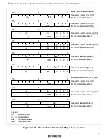


43
DDR7
←
0
DDR6
←
0
CCR(I)
←
0
Execute SLEEP instruction
Sleep mode
Program
execution state
(EN = 0)
Figure 2.14 Transition to Sleep Mode
Note: When sleep mode is entered, set DDR to 0 to use the pins as I/O input ports before
executing a SLEEP instruction. When writing to the DDR7 and DDR6 bits, use the
MOV instruction instead of the bit manipulation instruction.
2.8.3
Exit from Sleep Mode
Sleep mode is cleared by an input to the I/O-1/
IRQ
, I/O-2/
IRQ
, or
RES
pin.
1. Exit by interrupt
In sleep mode, the I/O-1/
IRQ
and I/O-2/
IRQ
pins can receive interrupt signals. When a high-
to-low transition occurs in the input, the external clock is supplied to the CPU and on-chip
modules, sleep mode is cleared, and interrupt exception handling starts. The external clock
must be stable when the interrupt signal goes low. Figure 2.15 shows the transition sequence
from sleep mode to interrupt handling. Figure 2.16 shows the timing of an interrupt in sleep
mode.
2. Exit by reset
If the
RES
input goes low during sleep mode, the external clock is supplied to the CPU and on-
chip peripheral modules. After that, when the
RES
input goes high, the CPU begins reset
exception handling. The
RES
input must be held low for at least 20 stable external clock
cycles.


