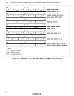


42
2.8
Power-Down State
2.8.1
Overview
The H8/3150 series has a sleep mode, a power-down state in which CPU functions are halted to
conserve power.
Table 2.14 summarizes the conditions for transition to sleep mode, the state of the CPU and on-
chip peripheral modules in sleep mode, and the conditions for exit from sleep mode.
Table 2.14
Power-Down State
States
Mode
Transition
Condition
CLK
CPU Clock
and CPU
CPU Reg's
RNG Clock
and RNG
RNG Reg's
Sleep
mode
Execute
SLEEP
instruction
0 MHz to t
cyc
*
Stop
Retained
Stop
Retained
States
Mode
WDT Clock
and WDT
WDT Reg's RAM
DR and
DDR
I/O Ports
ECR and
EPR
Exiting
Methods
Sleep
mode
Stop
Retained
Retained
Retained
Interrupt
input
Initial
values
Reset or
external
interrupt
Note: * For details on t
cyc
, see figures 12.1 and 12.5 in section 12, Electrical Characteristics.
2.8.2
Transition to Sleep Mode
Sleep mode is entered by executing the SLEEP instruction.
In sleep mode the CPU, clock, and on-chip functions halt, reducing power dissipation. As long as
the necessary voltage is supplied, however, the contents of CPU registers, RNG registers, WDT
registers, RAM, and I/O port registers (DR and DDR) are retained. The ECR and EPR in the
EEPROM are initialized. I/O-1/
IRQ
and I/O-2/
IRQ
become interrupt input pins. The I/O-1/
IRQ
,
I/O-2/
IRQ
, and
RES
signals must be kept high during sleep mode. If either one of I/O-1/
IRQ
and
I/O-2/
IRQ
is not used, the unused pin must be left as an input pin and left open (unconnected).
When the I/O-1/
IRQ
and I/O-2/
IRQ
are used as output pins, change them into input pins by
writing 0 to the DDR7 and DDR6 bits before executing the SLEEP instruction.
Figure 2.14 shows the sequence for transition to sleep mode.


