background image

5-1

5.1

Outline

This chapter provides troubleshooting flow charts and describes error messages.

5.2

Error Message

When no bearing pulse signal is input to the display unit, BP-SIG-MISS is indicated, and when no
heading signal, HD-SIG-MISS. Check the antenna cable when those indications appear.

Visual Alarms

Visual alarms appear on the display to alert the operator that the system is abnormal. The name and
meaning of each visual alarm is tabulated below.

Alarm Type

Visual Alarm

Description

LOST

No echo received from an acquired target for nine
consecutive sweeps. The target mark blinks.

TARGET FULL
(AUTO+MANU)

Relevant target memory becomes full.

ARPA alarm

GUARD

Target transits the operator-set guard ring.

HEAD LINE

No heading pulse to the SPU board

AZIMUTH

No bearing pulse to the SPU board.

TRIGGER

No trigger pulse to the SPU board

VIDEO

No video signal to the SPU board

LOG

No log signal contact closure to SPU board for one
minute

GYRO

No gyro signal AD format to SPU board for one minute

Input signal

(SIGNAL
MISSING)

EPFS

No L/L data from Electronic Position Fixing System to
the SPU board

5.3

Troubleshooting Flow Charts

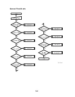
The troubleshooting flow charts help the service technician to diagnose a problem. To use the flow charts,
first find symptom and its flow chart number in the flow chart on the next page. Then, follow appropriate
flow chart to troubleshoot.

Chapter 5. TROUBLESHOOTING

Summary of Contents for FR-2155

Page 1: ...MARINE RADAR MODEL FR 2155 PRINTED IN JAPAN...

Page 2: ...p a n T e l e p h o n e 0 7 9 8 6 5 2 1 1 1 T e l e f a x 0 7 9 8 6 5 4 2 0 0 Y o u r L o c a l A g e n t D e a l e r A l l r i g h t s r e s e r v e d P U B N o S M E 3 4 6 7 0 A F R 2 1 5 5 K A O K...

Page 3: ......

Page 4: ......

Page 5: ......

Page 6: ...12 Echo averaging EAV 1 2 3 2 13 2 13 Echo Stretch 1 2 and Enhanced video 2 14 2 14 Memories Memory Frame Priority 2 15 2 15 Antenna on off Control 2 16 2 16 Check of ARP and RP board Connection 2 17...

Page 7: ...14P0298 3 9 Location of parts on INT Board 03P9252 3 10 Location of parts on GYRO Board 64P1106 3 11 Location of parts on PTU Board 03P9245 3 12 Location of parts on Power Supply Unit PSU 001 3 13 Lo...

Page 8: ...ED Status 4 3 4 4 Self test 4 7 4 5 Notice on Replacing Major Parts 4 9 4 6 Program Numbers 4 10 4 7 How to update system program 4 10 Chapter 5 TROUBLESHOOTING 5 1 Outline 5 1 5 2 Error Message 5 1 5...

Page 9: ...itor Control and Processor Units The figure shows the major configuration of FR 2155 Display Unit RDP 124 ARPA Board ARP 26 NAV IEC 61162 1 Input Output IEC 61162 1 Input Speed Log Option Performance...

Page 10: ...6 INT Board 03P9252 Mother Board 03P9251 ARP Board Optional ARP 26 18P9002 B RP Board Optional RP 26 14P0298 Card I F Board Optional RP 26 14P0299 PDM Board PDM 9025 Gyro Board Optional GC 8 64P1106 A...

Page 11: ...oard Name Type IF AMP Board 03P6734 C MODULATOR Board 03P6666 C PFN 1 Board 03P6668 PFN 2 Board 03P6669 B BEARING SIG GEN Board MP 3795 Magnetron M 4505 E INT Board 03P9004 Magnetron Current DET Board...

Page 12: ...pm 3 60 Hz DC approx 16 rpm 3 50 Hz Scanner Housing Structure Open Radiator Standard 1 65 m Compass Safe Distance Steering 1 25 m TRANSCEIVER ITEM FR 2155 Magnetron M 4505 E Frequency Modulation 9385...

Page 13: ...EC 61162 1 RATTM ARP 26 required RS 232C port input output J456 System program updating Gyro port input J446 AD100 format Speed Log port input J448 Contact closure signal Alarm output J452 12 V buzzer...

Page 14: ...ure Display Unit 15 deg to 55 deg Humidity Relative humidity 95 or less at 40 deg Vibration IEC 945 Edition 3 POWER SUPPLY POWER CONSUMPTION ITEM FR 2155 AC Power Supply 110 VAC 90 to 126 V 220 VAC 19...

Page 15: ...s is supplied to the display unit via the power supply unit PSU 001 Receiving 12 V from the display unit the relay in the PSU 001 is turned on and ship s mains is supplied to the power supply unit PSU...

Page 16: ...Board to the ARP 26 Board Heading Bearing pulse Video Trigger Bearing in AD format and Ship s speed in IEC 61162 Target acquision and tracking are performed on the ARP Board and displayed on the CRT...

Page 17: ...P RAM ARP Board 18P9002 SPD CRS D P RAM Scrolling VRAM AGDC CPU Multi plexer L L S C PWR Board 03P9245 Regulator Protector Overcurrent Detector Rectifier Ships Mains AC 100 110 115 V PM Board 03P9225...

Page 18: ...est ARP 23 hardware 2 Converts GAIN STC FTC and I R processed video signal to quantized video QV and sends back to the SPU Board 3 Performs automatic and manual target acquisition and tracking 4 Detec...

Page 19: ...connector for the RJ 8 4 Includes a connector for the control head GYRO CONVERTER Board 64P1106 1 Converts gyrocompass signal into AD format signal 2 Outputs Max 6 AD format signal 25 ms or 200 ms ju...

Page 20: ...enerated resulting in nothing on the screen 10 The bearing scale countdown indication etc appear 11 The screen is degaussed automatically 3 minute warm up can be skipped by pressing ENTER several time...

Page 21: ...OK No Yes Display radar picture radar signal processing ARPA 18P9002 Initializes NAIN CPU Initializes DSP RAM between MAIN CPU and SPU CR1 on pcb 18P9002 blinks Tx ON END Yes No Initializes DSP RAM be...

Page 22: ...U5 7 EEPROM U10 ACRTC U16 FR2115 SME 23 A22 A23 A24 R134 Trigger Gen Even Echo Handling Sampling I F Rejection Noise Rejection U44 03S9060 U72 VlEVEL 0 U73 VlEVEL 2 U74 VlEVEL 4 U75 VlEVEL 6 U76 VlEV...

Page 23: ...51 Video Amp GAIN A C SEA and A C RAIN Adjustment C14 about 4Vpp 03P9253 TP12 A18 P551 ARP Board TP6 FR 2155 SMJ10E about 4Vpp 2 6 Video Signal Flow The figure below shows video signal flow The video...

Page 24: ...s Video contrast menu selection about 4 0 Vpp 1 Mixer Q17 In A C AUTO mode the pulse whose level is the same as the main bang is mixed with the video signal The falling edge of the pulse is coincident...

Page 25: ...FWHG XOO VHDUFK 9DU LQJ WXQH FRQWURO YROWDJH 781 217 IURP DERXW 9 WR 9 WKH PD LPXP WXQH LQGLFDWRU YROWDJH LV IRXQG DQG WKDW WXQH FRQWURO YROWDJH D LV PHPRUL HG 6KRUW VHDUFK 7KH WXQH FRQWURO YROWDJH FK...

Page 26: ...cted In manual tuning mode the graphical tuning control voltage indicator appears under the tuning indicator The minimum scale is 2 V and the maximum scale is 32 V 2 11 Tuning Circuit Figure below sho...

Page 27: ...rnately appear and disappear on the screen Normally unstable echoes such as those from sea clutter and noise appear at random positions with every rotation of the antenna To distinguish real target ec...

Page 28: ...signal is integrated in the video amplifier 3 Enhanced video The echo is enlarged to increase the number of memories to be filled with the data a Minimum echo size one dot b Signal level 15 or more c...

Page 29: ...dots 2048 dots Cursor Characters Menu Data Mask Cursor Gyro U1 and U3 4 frames no frame ARPA Each 1 4 of U4 U6 U8 and U9 2 frames RP no frame data from RP Radar mark Radar map Each 3 4 of U4 and U6 3...

Page 30: ...6 9 K1 4 PTB 14 1 2 3 XK 1 PTB 12 Ship s Main DC24V MOTOR DTB 2 2 MOTOR SW STB 1 24 MOTOR SW 26 SW S801 12V SCANNER UNIT K2 THERMAL RELAY 24Vdc 2 15 Antenna Control Signal The SPU board generates ante...

Page 31: ...r functional differences are 1 Operational with 42 rpm scanner unit ARP 23 36 rpm 2 Scenario in compliance with HSC performance standards no scenario 3 A maximum of 3 reference targets one target 4 Va...

Page 32: ...gital Signal Processor BP 1 Target data of manually acquired target and automatic acquisition of target inside guard ring 2 Automatic tracking of target 3 Calculation of target s CPA TCPA speed and co...

Page 33: ...22 Latch U41 BP Counter Comparator A D Converter ROM U3 RAM U9 10 EEPROM U8 D P RAM U4 11 MAIN CPU U2 DIP SW S1 Status Switch for Error Detection U42 47 Echo Sampler To SPU Board s DP BUS CR1 Blinks...

Page 34: ...rocessor 3 The target must be within acquisition area 0 1 to 32 nm or 24 nm depending on initial setting Target echoes behind a land echo within the acquisition area cannot be acquired automatically 4...

Page 35: ...than 800 meters 2 Greater than 1200 meters 3 Greater than 1600 meters 4 No limit QV SELECT Requires no local adjustment however it judges whether an echo is land or not by painting echoes in varying i...

Page 36: ...K INPUT SIG CHECK 1 Keying sequence PLOT MENU 0 8 HD OK ERR No heading signal input to ARPA Board for 10 seconds BP OK ERR No bearing signal input to ARPABoard for 10 seconds T OK ERR No trigger signa...

Page 37: ...e does not change at the adjustment To check the front end rotate the gain control knob from fully cw to fully ccw and read the echo count If the number decreases the front end functions normal No 2 0...

Page 38: ...s memorized by the SPU board Figure 2 14 Block Diagram of RP Board FR2115 SME 18 Power Fail U15 DIP SW P F Activated by H CPU FR 30 U13 OSC 12 5 MHz U17 Dual Port RAM RAM 8 K bytes U4 Buffer U22 23 27...

Page 39: ...g 1 2 3 True echo trail ARP 26 J449 O Remote display R G B H SYNC V SYNC Monitor Printer Buffer Board 03P9229 required J450 I O Nav data NMEA0183 V2 0 Current Loop I Navaid GP 70MK2 GP 80 GP 500MK2 O...

Page 40: ...Data to be displayed Sentence O S Cursor Position RNG BRG to WPT SPD Water Temp Water Depth Water Current Date Time ARP 26 SPD ARP 26 External WPT BWC BWR X X DPT DBT DBK DBS X GGA GLL X VBW VHW X X M...

Page 41: ...racteristic Input of amplifier GAIN STC Not controlled BEARING Signal BP Pulse 360 pulses one ant rotation Polarity Voltage Positive 12 V Duty Cycle 50 20 HEADING Signal HD Polarity Voltage Negative 1...

Page 42: ...ideo signal 63 974 kHz 15 63 us 1696 dots 0 59 us 64 dots 11 80 us 1280 dots 1 18 us 128 dots 2 06 us 224 dots Video signal FR2115 SME 11 60 013 Hz 16 66 ms 1066 dots 16 us 1 dots 16 00 ms 1024 dots 4...

Page 43: ...justed by VR1 A rush current protector Q1 and R2 prevents rush current from being flow into smoothing capacitors C11 and C12 When the smoothing capacitors are charged to the rated voltage the main inv...

Page 44: ...oltage Detector U51 Voltage Protector Latch Q36 Main inverter 32 V CR52 24 V CR51 Chopper Control U92 Chopper CR94 Q97 Comparator Q94 F V Converter U93 Soft Start Control Overcurrent Detector U91 Chop...

Page 45: ...Read Sw S801 HD FL SYNC P Heading To dispaly unit discharge Pulse Transe T801 FR2155 SME 27A G0B8222 200VAC 3 50Hz 220VAC 3 60Hz RM 6585 24VDC K803 L K802 M2 K801 M1 PFN 2 Board 03P6669 B L801 CR813...

Page 46: ...602 IF Bandwidth CR611 612 Pre Amp Q609 Pre Amp Q601 Q608 MBS Generator U615 TP605 Video Amp Q605 to 607 U601 U602 U603 U604 U605 U606 TP601 U607 VC601 Log Amp U608 U609 U610 Q603 Q604 TP602 Tuning Am...

Page 47: ...positive going pul se is produced at pin 6 of U850 1 2 and sent to Q854 and then a negative going pulse is gen erated at the collector of Q854 The negative going pulse is differentiated by C866 and R...

Page 48: ...ettings Refer to the truth table shown below Pulselength P L B P L A K801 K802 K803 S L L OFF OFF OFF M1 L H ON OFF OFF M2 H L ON ON OFF L H H ON ON ON ON Short OFF open The circuit made up of K851 U8...

Page 49: ...n of the pulse is equal to the time required for the voltage wave to go and return in the L C network and it is given by the duration T 2N L C where N is the number of sections of the L C network CR80...

Page 50: ...ron heater when T801 secondary windings are unbalanced or the load is asymmetric Figure 2 19 Rising of pulse absorbed by Cr804 and CR815 Duplexer and mixer Since the radar system uses a single antenna...

Page 51: ...on signals from the magnetron and those received from other radars through the antenna and to protect the MIC Microwave IC The PIN diode has certain charac teristics as shown in Figure 2 20 and conduc...

Page 52: ...otates at a speed of 144 rpm between the two walls The photo transistor receives the light emitted by the light emitting diode thru a slit on the tim ing disc and converts it into electric current The...

Page 53: ...1 and R812 in the scanner unit especially when the cable is long TXHV is not generated when MAG ERROR signal is received from the transceiver unit A de fective magnetron and open circuit of the pulse...

Page 54: ...amplified and applied to the stack rectifier on the 03P6810 Board through power transformer T55 The TX HV of 780 V is adjusted by VR52 The following protectors are provided K51 Overcurrent detector fo...

Page 55: ...ard 03P6667 This board produces 12 V 12 V and magnetron heater voltage U1 is a voltage comparator and U3 is a switching regulator oscillating at 90 kHz U3 Q3 and CR7 compose voltage adjuster for the 1...

Page 56: ...th the relay K3 on ANT1 signal is generated at TX 0 V at TX and the relay K3 in the PSU 004 is turned on so that power is applied to the scanner motor The type of the thermal relay K2 must be selected...

Page 57: ...ort all supply lines to the chassis with an insulated screwdriver or a similar tool before touching the circuit Working on the Scanner Unit Mast Work on the scanner unit mast is dangerous and doubly s...

Page 58: ...nt Display Unit Location of Major parts Figure 3 1 Display Unit front view Figure 3 2 Display Unit inside view Control panel Handle Stay This cover is removed to gain access to SPU ARP and RP Boards D...

Page 59: ...PU Board 03P9253 ARP Board 18P9002B RP Board 14P0298 GC 8 Board 64P1106 DTB 2 T B Mother Board 03P9251 INT Board 03P9252 SPU Board Video Level Adjuster R140 Fuse for P M F402 0 5 A Fuse for P M F401 0...

Page 60: ...3 4 Figure 3 5 Display Unit top view drawing forward Figure 3 6 Display pedestal for side shield cover removed PTU Board 03P9245 Shield cover removed Power Switch for Maintenance Fuse F1 Fuse F2...

Page 61: ...A10 Board UBH188 VIDEO Board PBH173 SOCKET Board UBH182 DEGAUSS Board PDM9025 INT Board PBH183 0 HPOSI Under the cover MAIN Board PBH172 0 CRT ADJ Board PBH132 1 HV ADJ 1 Press the ADJ or ADJ button o...

Page 62: ...necessary How to change meun setting to default Keep pressing the MENU button until UTILITY MOD menu appears Press SEL once to select INITIALIZE Press MENU Within 5 seconds after the message INITIALIZ...

Page 63: ...xcept for maximum range TP7 H SYNC Approx 64 kHz TP8 V SYNC Approx 60 Hz TP9 TUNE V Approx 2 V to 32 V TX TP11 VIDEO Approx 5 V TX TP12 VIDEO LEVEL 3 9 to 4 1 Vpp negative main bang level Adjusted by...

Page 64: ...pprox 10 to 12 V TP5 VIDEO INPUT Approx 4 5 Vpp TP6 OFFSET TP7 OFFSET 0 09 to 0 13 VDC adjusted by R104 TX TP8 GND TP9 QV OUTPUT Approx 4 V main bang level TP10 5 V 4 8 to 5 2 V TP11 12 V 11 0 to 13 0...

Page 65: ...3 9 Location of Parts on RP Board 14P0298 CR1 S1 Battery BT1 Flash ROM U3...

Page 66: ...t Approx 4 Vpp TP4 ANALOG Input Same as output of connected equipment TP5 GND TP6 VIDEO Output 3 9 to 4 1 Vpp main bang level RF video output adjusted by R21 EXT video output adjusted by R134 Selected...

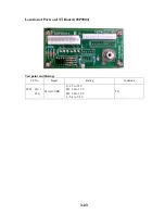
Page 67: ...11 Location of Parts on GYRO Board 64P1106 Test points and Ratings TP No Signal Rating Condition TP1 5 V 5 19 to 5 21 VDC adjusted by R42 JP1 F1 F2 F3 F4 CR21 JP7 JP3 JP5 JP2 JP4 R42 CR22 TP1 JP8 BT1...

Page 68: ...35 0 VDC TX J105 2 7 12 V 12 1 to 13 5 VDC J105 4 7 5 V 4 8 to 5 2 VDC J105 9 7 12 V 11 0 to 13 0 VDC Q31 Collector Chassis Inverter freq U31 42 75 to 47 25 kHz adjusted by VR1 FL71 Chassis Inverter f...

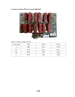
Page 69: ...t PSU 001 TX HV POWER SUPPLY 2 03P6680 Transformer T804 CHECK METER De icer Power SW S801 HOUR METER Fuse F801 5A Fuse F802 2A Fuse F803 2A TX HV POWER SUPPLY 1 03P6810 POWER SUPPLY 03P6667 FAN MOTOR...

Page 70: ...TP No Signal Rating Condition J2 1 12 V 3 GND 12 V 11 9 to 12 1 V adjusted by VR1 J2 2 12 V 3 GND 12 V 11 7 to 12 3 V TP1 24 V 20 to 42 V TP2 GND TP3 10 V 8 5 to 11 5 V TP4 Switching Freq 72 to 108 kH...

Page 71: ...3 15 Location of Parts on INT Board 03P9003 Test point and Ratings TP No Signal Rating Condition PTB 2 7 8 HEATER 8 2 to 8 8 V adjusted by R813 ST BY 0 25NM PTB 2 R813...

Page 72: ...3 16 Location of Parts on TX HV Power Supply Board 1 03P6810 Test point and Ratings TP No Signal Rating Condition J5 1 2 TX HV 780 to 800 VDC TX 48NM Rating for Check Meter TX HV 0 55 to 0 75 J5...

Page 73: ...ondition TP51 TP52 12 V 10 8 to 13 2 V TP53 TP52 Switching Freq 54 to 57 s 17 5 to 18 5 kHz adjusted by VR51 TP54 TP52 Switching Freq 54 to 57 s 17 5 to 18 5 kHz adjusted by VR51 ST BY 0 25NM Input Vo...

Page 74: ...3 18 Location of Parts on Power Supply Unit PSU 004 PTB 12 PTB 14 PTB 11 PTB 13 Fuse F1 10A Fuse F2 10A Fuse F3 2A THERMAL RELAY K2 RELAY Under Side K3 RELAY Board 03P9146 RELAY K1...

Page 75: ...0049 0050 Scanner Unit side view cover removed Scanner Unit stern side cover removed Scanner Unit stern side cover and RF Unit removed RF Unit RTR 030 R812 R811 Scanner Motor Reed switch Bearing SIG G...

Page 76: ...Pulse Transformer RT 9028 TR Limitter BS4112 E3902 MIC SRX 24 MIC INT Board MIC 6550 INT Board 03P9004 Modulator Board 03P6666C Circulator RC 3686 IF Amp Board 03P6734C PFN 2 Board 03P6669 PFN 1 Boar...

Page 77: ...ion TP1 TP2 TRIGGER TP1 TP2 TRIGGER TRIGGER S 380 to 400 s Adjusted by VR858 M1 470 to 600 s M2 840 to 1000 s L 1250 to 1600 s TX Removed Fuse F801 for PSU 001 Unit TP3 Chassis TRIGGER 0V V1 T V2 T 0...

Page 78: ...point and Ratings TP No Signal Rating Condition TP604 DI MONITOR 1 9 to 2 1VDC Adjusted VR602 ST BY 0 25 NM J604 3 8 TUNING PRESET Adjusted by VR601 so that maximum echoes on the screen with maximum l...

Page 79: ...3 23 Location of Parts on INT Board 03P9004 Test point and Ratings TP No Signal Rating Condition J823 8 9 MAG CURR S 2 5 to 5 5 V M1 3 0 to 5 5 V M2 5 0 to 7 0 V L 5 4 to 7 8 V TX...

Page 80: ...3 24 Location of Parts on PFN 1 board 03P6668...

Page 81: ...3 25 Location of Parts PFN 2 board 03P6669 RELAY Condition K801 802 803 Pulse length K801 K802 K803 S Open Open Open M1 Short Open Open M2 Short Short Open L Short Short Short...

Page 82: ...ort all supply lines to the chassis with an insulated screwdriver or a similar tool before touching the circuit Working on the Scanner Unit Mast Work on the scanner unit mast is dangerous and doubly s...

Page 83: ...F 2 Not used OFF 3 Not used OFF 4 Not used OFF S1 Description Default 1 Baud rate of ARPA output data OFF 4800 bps ON 9600 bps OFF 2 Tracking model OFF A TRK 88 ON A TRK 94 OFF 3 Not used OFF 4 EEPROM...

Page 84: ...No JP92 No R98 4 7 k ohms 03P9245D PTU Board AC 220 VAC 24 rpm JP1 No JP2 No JP3 No JP4 Yes JP91 No JP92 No R98 4 7 k ohms INS RX C fromat J468 J1 J2 INS RX H fromat J469 J1 J2 J1 J2 Current loop J3 J...

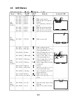
Page 85: ...arm TRIG freq TRIG freq GYRO alarm LOG alarm DSP FLK FE echo data or or Blinks at irregular interval Lights if heading data is not re ceived for more than 10 sec Lights if bearing data is not re ceive...

Page 86: ......

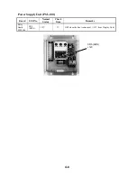
Page 87: ...4 6 Power Supply Unit PSU 001 Board LED No Normal Status Check Item Remarks Relay Board 03P9146 CR5 GRN 12V OFF when the line is abnormal 12V from Display Unit CR5 GRN 12V...

Page 88: ...OK 1234 ARP 1859038104 OK OK OK 0000 DSP 1859039101 OK OK OK RP 0359150101 OK OK OK 0000 DRAM OK RP BOARD BAT OK RP CARD 1 OK CARD 2 OK CARD 1 BAT OK CARD2 BAT OK ANTENNA SPEED 0 0RPM TRIG FREQ 0Hz M...

Page 89: ...y Xs 2 RAM card will be NG if the card is inserted after power up 3 RP BOARD BAT Checks the voltage of the battery on the RP board NG will appear when the battery drops to less than 2 65 V The capacit...

Page 90: ...n is fitted turn on the power and measure magnetron current See Chapter 3 for heater voltage rating and potentiometer to be adjusted 5 Allow at least 30 minutes under ST BY for pre heating 6 Transmit...

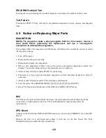
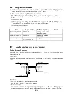
Page 91: ...oard 03P9253 0359149101 Loading program with a personal computer RP Board 03P0298 0359150101 Loading from program master card ARP Board 18P9002 ARP 18590381XX DSP 18590391XX Changing PROM 4 7 How to u...

Page 92: ...P 2 xxxxxxxx Byte transfer bps xxxxxxxx Now Erasing xxx percent completed FR2115 SME 46B RP Program The program is stored onto the flash ROM U3 on the RP board 1 Insert the program card into the upper...

Page 93: ...LL AUTO MANU Relevant target memory becomes full ARPA alarm GUARD Target transits the operator set guard ring HEAD LINE No heading pulse to the SPU board AZIMUTH No bearing pulse to the SPU board TRIG...

Page 94: ...NG OK No GAIN STC FTC effect Flow chart 9 NG OK No heading data Flow chart 3 NG OK Key s inoperative Flow chart 5 NG OK Abnormal display Flow chart 2 NG OK Poor sensitivity Flow chart 8 NG OK No targe...

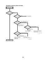
Page 95: ...pe CDT2163B Defective 140 Vdc line See block diagram of SPU board Confirm that maintenance SW is on OK NG set to front side Rating OK set to rear side Check input voltage at DTB 1 Turn on w mainte sw...

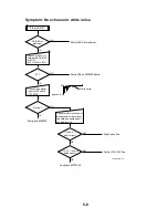
Page 96: ...CRT brilliance NG OK OK OK Picture is in sync NG Focus Picture size End See block diagram of SPU board Defective 03P9253 SPU Picture is synchronized automatically No adjuster NG OK NG Adjust CRT focus...

Page 97: ...low chart 3 Heading data indication Blank OK Normal Power OFF and ON OK Heading data from the sensor temporarily interrupted Check CLK data at INT board J446 3 4 OK OK Faulty heading sensor or its int...

Page 98: ...or blank Some data shown by asteriska or blank OK OK NG Wrong data sentence format selection Select correct sentence Check nav equipment s output sentences OK OK NG Faulty pcb 03P9253 or IEC61162 not...

Page 99: ...one key is faulty ALL keys Single vertical row only Single vertical row of keys is faulty Faulty pcb 03P9253 Faulty S1 to S11 on pcb 03P9255 S1 to S19 on pcb 03P9256 Defective signal line Faulty pcb 0...

Page 100: ...y PTU Board Faulty Ant SW on 03P9254 Faulty 03P9253 Flow chart 6 NG Antenna does not rotate ON ANT SW position 12 V PTB 13 4 when TX key is pressed OFF PTB 13 4 on PSU 004 Turn on the SW FR2155 SME 70...

Page 101: ...OK Faulty pcb 03P9253 Set GAIN VR at maximum NG Faulty VR4 on 03P9255 Board NG Open or short circuit OK 12 12V line on antenna unit OK Check for short circuited or disconnected video signal line betw...

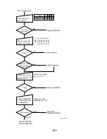
Page 102: ...al mode about 1 to 3 V In manual mode rotate TUNE VR NG Poor sensitivity NG No TX trigger Faulty pcb 03P9253 NG Faulty pcb 03P9253 0V approx 12V Replace magnetron To 1 page 5 11 OK Faulty pcb 03P9253...

Page 103: ...about 2 to 32 V Manual tune IND voltage about 1 to 3V NG NG NG Faulty pcb 03P9253 NG about 1V Faulty pcb 03P9253 Replace magnetron From 1 on page 5 10 FR2155 SME 66 Check TUNE IND voltage in self tes...

Page 104: ...From 2 on page 5 10 FR2155 SME 67 Faulty TX HV 03P6810 L 4 5V to 5 0 Vdc ST BY 7 0 V to 7 5 Vdc Rating OK NG Faulty magnetron L 5 4 V to 7 8 Vdc NG Faulty pcb 03P6667 ST BY 780 Vdc to 800 Vdc TX 0 Vdc...

Page 105: ...G OK A C RAIN can be adjusted OK End Faulty pcb 03P9253 Faulty VR4 on 03P9255 board MIN approx 7 V MAX approx 0 V OK Check voltage at U49 14 on 03P9253 NG Faulty pcb 03P9253 MIN approx 0 V MAX approx...

Page 106: ...ect 25 msec AD format ARP DSP is NG H B T and or V is NG 0 or no change All targer not acquired Faulty pcb 18P9002 Faulty pcb 18P9002 Faulty pcb 18P9002 E PA When CR1 on ARP board is off faulty 18P900...

Page 107: ......

Page 108: ......

Page 109: ......

Page 110: ......

Page 111: ......

Page 112: ......

Page 113: ......

Page 114: ......

Page 115: ......

Page 116: ......

Page 117: ......

Page 118: ......

Page 119: ......

Page 120: ...03P9252 1 4 03P9252 2 4 03P9252 3 4 03P9252 4 4 03P9251 03P9251 PDM9025 HV 9017 03P9245 AC 03P9246 DC PBH172 PBH173 UBH188 A00010 UBH182 A00010 UBH207 A00010 64P1106 1 2 64P1106 2 2 03P9225 03P9229 0...

Page 121: ......

Page 122: ......

Page 123: ......

Page 124: ......

Page 125: ......

Page 126: ......

Page 127: ......

Page 128: ......

Page 129: ......

Page 130: ......

Page 131: ......

Page 132: ......

Page 133: ......

Page 134: ......

Page 135: ......

Page 136: ......

Page 137: ......

Page 138: ......

Page 139: ......

Page 140: ......

Page 141: ......

Page 142: ......

Page 143: ......

Page 144: ......

Page 145: ......

Page 146: ......

Page 147: ......

Page 148: ......

Page 149: ......

Page 150: ......

Page 151: ......

Page 152: ......

Reviews: