


C156-E097-01EN
xv
FIGURES
page
1.1
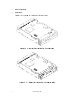
MCE3064SS/MCF3064SS outer view (with panel).............................................................1 - 6
1.2
MCE3064SS/MCF3064SS outer view (without panel) .......................................................1 - 6
1.3
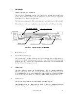
Optical disk drive configuration ...........................................................................................1 - 7
1.4
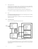
Control circuit section block diagram ..................................................................................1 - 8
1.5
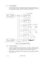
System configuration example ............................................................................................1 - 10
2.1
Optical disk cartridge............................................................................................................2 - 16
2.2
Algorithms for alternate processing ....................................................................................2 - 20
2.3
Example of alternate processing...........................................................................................2 - 21
3.1
Surface temperature measurement points.............................................................................3 - 2
3.2
Dimensions ...........................................................................................................................3 - 5
3.3
Dimensions (without panel)..................................................................................................3 - 6
3.4
Installation directions ...........................................................................................................3 - 7
3.5
Centers of gravity..................................................................................................................3 - 8
3.6
Mounting frame structure .....................................................................................................3 - 9
3.7
Service clearance ..................................................................................................................3 - 10
3.8
Current waveform (+5 VDC)................................................................................................3 - 11
3.9
Power on/off sequence (1) ....................................................................................................3 - 11
3.10
Power on/off sequence (2) ....................................................................................................3 - 12
3.11
Power on/off sequence (3) ....................................................................................................3 - 12
3.12
AC noise filter (recommended) ............................................................................................3 - 13
3.13
Connector and terminal locations .........................................................................................3 - 14
3.14
Power supply connector........................................................................................................3 - 15
3.15
SCSI interface connector (drive side)...................................................................................3 - 15
3.16
Cable connection mode.........................................................................................................3 - 17
3.17
SCSI cable connector............................................................................................................3 - 19
3.18
SCSI cable connection..........................................................................................................3 - 21
3.19
External operator panel circuit example...............................................................................3 - 23
3.20
External operator panel interface connector.........................................................................3 - 24
4.1
Packaging style .....................................................................................................................4 - 3
4.2
SCSI bus connection modes ................................................................................................4 - 4
4.3
Positions of setting terminals and switches ..........................................................................4 - 6
4.4
Setting switch (SW1) ............................................................................................................4 - 7
Summary of Contents for MCE3064SS
Page 1: ...C156 E097 01EN MCE3064SS MCF3064SS OPTICAL DISK DRIVES PRODUCT MANUAL ...
Page 3: ...This page is intentionally left blank ...
Page 31: ...This page is intentionally left blank ...
Page 52: ...C156 E097 01EN 2 21 Figure 2 3 Example of alternate processing ...
Page 53: ...This page is intentionally left blank ...
Page 72: ...C156 E097 01EN 3 19 Figure 3 17 SCSI cable connector ...
Page 81: ...This page is intentionally left blank ...
Page 97: ...4 16 C156 E097 01EN Figure 4 5 SCSI connection check 2 ...
Page 99: ...This page is intentionally left blank ...
Page 113: ...This page is intentinally left blank ...
Page 119: ...7 2 C156 E097 01EN Host system A Host system B Figure 7 1 Example of SCSI configuration ...
Page 133: ...7 16 C156 E097 01EN Figure 7 6 ARBITRATION phase ...
Page 135: ...7 18 C156 E097 01EN µ Figure 7 7 SELECTION phase 30 30 30 30 ...
Page 141: ...7 24 C156 E097 01EN Figure 7 10 Transfer in asynchronous mode 18 18 ...
Page 145: ...7 28 C156 E097 01EN Figure 7 11 Transfer in synchronous mode 11 11 11 11 43 18 43 18 ...
Page 146: ...C156 E097 01EN 7 29 Figure 7 12 Transfer in FAST SCSI mode ...
Page 148: ...C156 E097 01EN 7 31 Figure 7 13 Data transfer rate in asynchronous mode ...
Page 158: ...C156 E097 01EN 7 41 Figure 7 17 RESET condition ...
Page 160: ...C156 E097 01EN 7 43 Figure 7 18 Bus phase sequence 1 of 2 ...
Page 161: ...7 44 C156 E097 01EN Figure 7 18 Bus phase sequence 2 of 2 ...
Page 167: ...This page is intentionally left blank ...
Page 171: ...This page is intentionally left blank ...
Page 181: ......


