PSoC® 4100S Pioneer Kit Guide, Doc. # 002-14067 Rev. *C
44
reduced time-to-market. It contains Cypress’s PRoC BLE device, two crystals, chip antenna, shield,
and passive components. For more information on using the EZ-BLE PRoC module, see
Using EZ-
BLE PRoC Module on page 46
.
A.2.15
External Crystals
The PSoC 4100S Pioneer Kit includes a 32.768-kHz (Y1) external crystal for the WCO input. The
WCO is used to provide an accurate low-frequency clock to PSoC 4100S for Deep-Sleep wake up
intervals, and WDT reset intervals.
A.3
Using the FM24V10 F-RAM
The PSoC 4100S Pioneer Kit has an onboard F-RAM chip that can hold up to 1 Mb of data. The chip
provides an I2C communication interface for data access. It is hard-wired to the I2C interface (P3[0]
and P3[1] of the PSoC 4100S); the same lines are routed to the KitProg2 I2C interface. Because the
F-RAM device is an I2C slave, it can be accessed or shared among various I2C masters on the
same lines. For more details on the F-RAM device, refer to the device
datasheet
.
A.3.1
Address Selection
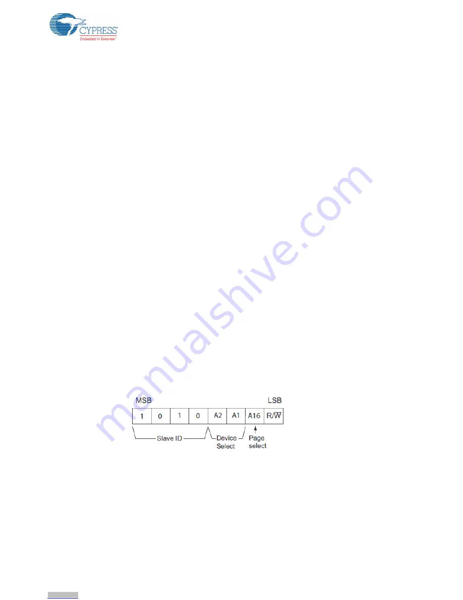
The slave address of the F-RAM device consists of three parts, as shown in
Figure A-9
: slave ID,
device select, and page select. Slave ID is an F-RAM family-specific ID provided in the datasheet of
the particular F-RAM device. For the device used on the PSoC 4100S Pioneer Kit (FM24V10-G), the
slave ID is 1010b. Device select bits are set using the two physical pins A2 and A1 in the device. The
setting of these two pins in PSoC 4100S Pioneer Kit is controlled by resistors R68/R71 (A1) and
R67/R70 (A2). Because the memory location in F-RAM is divided into two pages of 64 KB each, the
page select bit is used to refer to one of the two pages in which the read or write operations will take
place.
Note:
The 8-pin SOIC footprint provided for the F-RAM FM24V10 on the PSoC 4100S Pioneer Kit is
compatible with all I2C-based F-RAM devices from Cypress (FM24Vxx, FM24CLxx, and CY15BxxxJ
parts). F-RAM devices with more than 64 KB support only four addresses (four devices of the same
type on the same I2C bus); resistors connected to A1 (R68/R71)) and A2 (R67/R70) pins can be
used to select any of the four addresses. F-RAM devices with less than 64 KB and FM24CLxx parts
support eight addresses; resistors connected to A0 (R69/R72), A1 (R68/R71)) and A2 (R67/R70)
pins can be used to select one of the eight addresses.
Figure A-9. F-RAM I2C Address Byte Structure
A.3.2
High-Speed Mode (Hs-mode)
The FM24V10 supports a 3.4 MHz high-speed mode. A master code (00001XXXb) must be issued
to place the device into high-speed mode. Communication between master and slave will then be
enabled for speeds up to 3.4 MHz. A STOP condition will exit Hs-mode. Single-byte and multiple-
byte reads and writes are supported.
Downloaded from
Downloaded from
Downloaded from
Downloaded from
Downloaded from
Downloaded from
Downloaded from
Downloaded from
Downloaded from
Downloaded from
Downloaded from
Downloaded from
Downloaded from
Downloaded from
Downloaded from
Downloaded from
Downloaded from
Downloaded from
Downloaded from
Downloaded from
Downloaded from
Downloaded from
Downloaded from
Downloaded from
Downloaded from
Downloaded from
Downloaded from
Downloaded from
Downloaded from
Downloaded from
Downloaded from
Downloaded from
Downloaded from
Downloaded from
Downloaded from
Downloaded from
Downloaded from
Downloaded from
Downloaded from
Downloaded from
Downloaded from
Downloaded from
Downloaded from
Downloaded from


