


IV
- 32
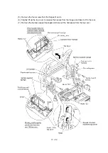
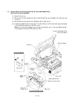
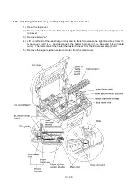
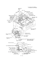
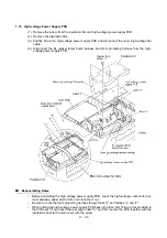
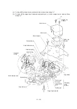
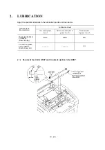
1.14 Main PCB
(1) For the FAX-8650P, take the battery ASSY*
1
out of the supports at the rear of the main cover.
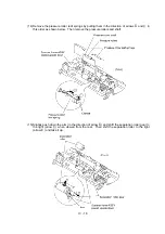
(2) Remove the screw from the main PCB.
(3) Slightly lift up the main PCB and disconnect it from the low-voltage power supply PCB.
(4) Disconnect the following harnesses from the main PCB:
• Speaker harness (2-pin, P7)
• Laser diode harness (5-pin, P6)
• Toner sensor harness (4-pin, P5)
• Polygon motor flat cable (5-pin, P4)
• NCU harness 2 (6-pin, P13)
• NCU harness (12-pin, P14)
• Solenoid harness (blue) (2-pin, P8)
• Hook switch harness*
2
(red) (2-pin, P9)
• Main motor harness (6-pin, P16)
• High-voltage power supply harness (12-pin, P20)
• Fan harness (2-pin, P3)
• CIS harness (7-pin, P19)
• Scanner motor harness (5-pin, P17)
• Panel-main harness (6-pin, P21)
(*
2
Not provided on the FAX-8650P.)
*
1
The FAX-8650P has a Ni-MH battery ASSY. Only when you need to replace the main PCB,
disconnect the battery harness. After installing a new main PCB, you may need to make
settings (e.g., calendar clock and voice messages) to be stored in the RAM. If you need to
replace the battery ASSY, do not disconnect the harness in this disassembly step. Doing so
with the power cord unplugged will lose the settings stored in the RAM. Refer to Section 1.1.
n
n
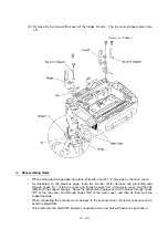
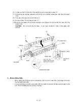
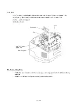
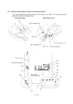
Reassembling Notes
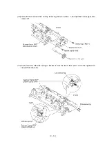
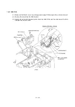
•
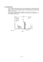
Route the hook switch harness (red), solenoid harness (blue), and main motor harness through
three latches "w," "y" and "z."
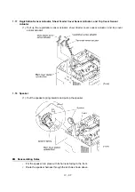
•
At the rear side of the main cover, route the harnesses as shown on the next page. Hook the
speaker harness on the left-hand battery support. For the FAX-8650P, route the battery
harness as shown on the next page to hold the three harnesses (scanner motor harness, CIS
harness and speaker harness) for preventing the battery harness from interfering with the top
cover sensor actuator.
•
Tape the CIS harness and panel-main harness at location "a" and tape the scanner motor at
location "b" as shown on the next page.
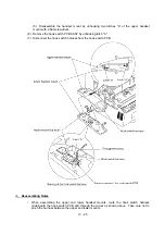
•
For the FAX-8650P, when transporting the main PCB, be sure to remove the battery ASSY (Ni-
MH battery) from the PCB. Failure to do so may result in a short circuit, overcurrent flow or
fire.
•
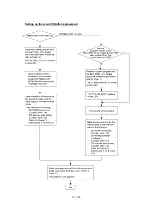
After you replace the main PCB, be sure to follow the flowchart given on page IV-34.
Summary of Contents for FAX-8650P
Page 1: ...FACSIMILE EQUIPMENT SERVICE MANUAL MODEL FAX3750 FAX 8650P MFC7750 ...
Page 5: ...CHAPTER I GENERAL DESCRIPTION ...
Page 12: ...CHAPTER II INSTALLATION ...
Page 13: ...CONTENTS 1 INSTALLING THE UPDATE DATA TO THE FACSIMILE EQUIPMENT II 1 ...
Page 16: ...CHAPTER III THEORY OF OPERATION ...
Page 18: ...III 1 1 OVERVIEW Not provided on the FAX 8650P ...
Page 28: ...III 11 Not provided on the FAX 8650P Location of Sensors and Actuators ...
Page 31: ...III 14 Main PCB Modem PCB ...
Page 36: ...CHAPTER IV DISASSEMBLY REASSEMBLY AND LUBRICATION ...
Page 42: ...IV 4 n n Disassembly Order Flow ...
Page 71: ...IV 33 1 Provided on the FAX 8650P 2 Not provided on the FAX 8650P ...
Page 72: ...IV 34 Setting up the main PCB after replacement ...
Page 84: ...IV 46 2 Control panel locks 3 Scanner frame ASSY and separation roller gear ...
Page 85: ...IV 47 4 Top cover lock spring 5 Gear drive unit ...
Page 86: ...CHAPTER V MAINTENANCE MODE ...
Page 93: ...V 6 Scanning Compensation Data List ...
Page 141: ...V 54 FAX3750 FAX 8650P MFC7750 Key Button Entry Order ...
Page 146: ...CHAPTER VI ERROR INDICATION AND TROUBLESHOOTING ...
Page 171: ...Oct 98 SM5X5303 Printed in Japan ...
Page 172: ...FAX3750 FAX 8650P MFC7750 Appendix 1 EEPROM Customizing Codes ...
Page 194: ......
Page 195: ......
Page 196: ......


