


• An
images.txt
file that defines the
.axf
files that the MCC loads into external memory during
configuration:
• An application note
.txt
file that defines:
— The number of FPGAs on the board.
— The number of oscillators and their frequencies.
— FPGA image file.
— Details of the SCC registers.
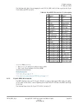
The following example shows a typical MPS3 board configuration
board.txt
file.
BOARD: HBI0309B
TITLE: Motherboard configuration file
[MCCS]
MBBIOS mbb_v132.ebf ;MB BIOS IMAGE
[APPLICATION NOTE] ;Please select the required processor
APPFILE: AN524\an524_v1.txt ;AN524 Cortex M33 SSE200 Subsystem for MPS3
The following example shows a typical MPS3 board configuration application note
.txt
file.
BOARD: HBI0309
TITLE: AN524 application note configuration file
[FPGAS]
TOTALFPGAS: 1 ;Total Number of FPGAS
F0FILE: an524_v1.bit ;FPGA0 Filename
F0MODE: FPGA ;FPGA0 Programming Mode
[OSCCLKS]
TOTALOSCCLKS: 7
;Clock generators OSC1 to OSC5 connect to FPGA top level signals
;OSCCLK[1] to OSCCLK[5] respectively.
;Clockgen OSC0 Drives XTAL1/CLKIN of LAN9220 Ethernet controller.
;FPGA top level signal OSCCLK[0] is driven by a fixed 24MHz reference.
;Clockgen OSC0 does not connect to FPGA top level signal OSCCLK[0].
;Clockgen OSC6 drives the DDR reference clock c0_sys_clk_p/n.
OSC0: 25.0 ; Ethernet reference 25MHz
; 24.0 OSCCLK[0] - refclk
OSC1: 32.0 ; OSCCLK[1] - ACLK
OSC2: 50.0 ; OSCCLK[2] - MCLK
OSC3: 50.0 ; OSCCLK[3] - GPUCLK
OSC4: 24.576 ; OSCCLK[4] - AUDCLK
OSC5: 23.75.0 ; OSCCLK[5] - HDLCD (MCC overrides this value)
OSC6: 100.0 ; GTX clock (DDR)
[HARDWARE CONTROL]
ASSERTNPOR: TRUE ;External resets assert nPOR
LEGACYRST: FALSE ;Legacy CB_nPOR/CB_nRST reset mode
CPUWAIT: 0x00000002 ;CPUWAIT value, set to 0xFFFFFFFF when using CB_nRST
[PERIPHERAL SUPPORT]
FPGA_SMB: TRUE ;SMB interface is supported (MCC_SMC<>FPGA_SMB)
FPGA_SCC: TRUE ;SCC interface is supported
SCCREG: 0x05300000 ;SCC registers base address
FPGA_DDR: TRUE ;DDR interface is supported
DDRBASE: 0x05208000 ;DDR I2C register address
FPGA_SYSREG: TRUE ;System register interface is supported
FPGAREG: 0x05302000 ;System registers base address
FPGA_REMAP: TRUE ;REMAP interface is supported
REMAPREG: 0x05300000 ;REMAP register address
REMAP: BRAM ;REMAP boot device BRAM/DDR/QSPI
REMAPVAL: 0 ;REMAP register value e.g. 0-BRAM. 1-QSPI
FPGA_HDMI: FALSE ;HDMI interface is supported
HDMIBASE: 0x05207000 ;HDMI I2C register address
FPGA_LAN: TRUE ;LAN LAN9220 interface is supported
LANBASE: 0x05400000 ;LAN LAN9220 base address
FPGA_RTC: TRUE ;RTC PL031 interface is supported
RTCBASE: 0x0530B000 ;RTC PL031 base address
FPGA_QSPI: TRUE ;QSPI interface is supported
3 Configuration
3.5 Configuration files
100765_0000_04_en
Copyright © 2017–2020 Arm Limited or its affiliates. All rights
reserved.
3-65
Non-Confidential