


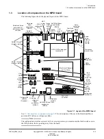


1.3
Location of components on the MPS3 board
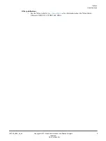
The following figure shows the physical layout of the MPS3 board.
3V battery
Configuration
microSD
card
FMC-HPC
connector
J25
J30
J33
J36
J26
J29
J35
J39
J27
J37
Shield 0
interface
Shield 1
interface
1
1
UL0
UL7
User
LEDs
1
8
7
6
5
4
3
2
User
switches
User
push
buttons
PB1 PB2
1
1
1
1
Xilinx Kintex Ultrascale
KU115 FPGA
Hardware
Reset
push button
(PBRST)
On/Off Soft Reset
push button
(PBON)
User
microSD
card
12V
DC IN
Audio
connectors
stacked
stereo
jacks
Combined
Ethernet and
dual-USB
HDMI
Debug
USB 2.0
FMC
Configuration
(Reserved)
Pmod0/1
interface
Pmod2/3
interface
Shield 0
configuration
Shield 1
configuration
38-pin
MICTOR
20-pin
IDC
DDR4
SODIMM
QVGA CLCD display and
touchscreen
20-pin
Cortex
and debug
10-pin IDC
14-pin
F-JTAG
ILA
FPGA
configuration
LED
Hardware
Reset
push button
(PBRST)
On/Off Soft Reset
push button
(PBON)
MCC
active
LED
Debug
USB
active
LED
PWR ON
3V3 OK
12V OK
System
LEDs
User
LEDs
PB1LED
PB2LED
Configuration
switches
(Reserved)
J58
J59
Microphone
bias user-links
L R
Shield and Pmod
power and I/O
reference voltage
user links
J24
J28
J34
J38
Figure 1-1 Layout of the MPS3 board
for a description of the use of the Shield and Pmod
power and I/O reference voltage user links.
Note
The configuration switches are reserved. For correct operation, you must ensure that both switches are in
the OFF position, that is, pointing away from the board.
1 Introduction
1.3 Location of components on the MPS3 board
100765_0000_04_en
Copyright © 2017–2020 Arm Limited or its affiliates. All rights
reserved.
1-15
Non-Confidential