


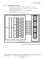


Forming the 32-bit address in the FPGA
The FPGA design must form the 32
‑
bit address, for AHB
‑
type transfers inside the FPGA, from
the following:
• The least significant bit (LSB), generated by the FPGA design.
Note
The MCC-SMC interface supports only four
‑
byte address mode transactions. To support
four
‑
byte address mode, the LSB generated by the FPGA design must be
0b0
and the LSB of
the MCC-SMC interface is always
0b0
.
• 25 address bits from the MCC.
• Six user bits, generated by the FPGA design.
The MCC can access 64MB of user memory for each Chip
‑
Select, that is, a total memory space
of 256MB. Each Chip
‑
Select can point to non
‑
contiguous areas in the user design. But the total
amount of user memory that each Chip
‑
Select accesses cannot exceed 64MB.
The six address bits generated by the design, and if necessary, the Chip
‑
Select bits, define which
parts of the user memory space are accessed.
The following figure shows the formation of the AHB 32
‑
bit address in the FPGA.
31
1 0
6 user bits
0
26 25
User bits generated
by FPGA design from
Chip-Selects and user
defined offsets
LSB generated
by FPGA design
SMBM_A[24:16],SMBM_D[15:0]
Figure 2-11 Formation of 32-bit address in FPGA
2 Hardware description
2.7 MCC-SMC interface
100765_0000_04_en
Copyright © 2017–2020 Arm Limited or its affiliates. All rights
reserved.
2-32
Non-Confidential