


A96G140/A96G148/A96A148 User’s manual
20 Development tools
259
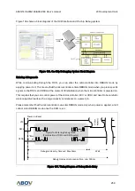
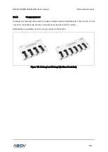
Figure 136 shows a block diagram of the OCD interface and On-chip Debug system.
Figure 136. On-Chip Debugging System Block Diagram
Entering debug mode
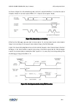
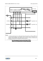
While communicating through the OCD, you can enter the microcontroller into DEBUG mode by
applying power to it. This means that the microcontroller enters DEBUG mode when you place specific
signals to the DSCL and DSDA at the moment of initialization when the microcontroller is powered on.
This requires that you can control power of the microcontroller (VCC or VDD) and need to be careful to
place capacitive loads such as large capacity condensers on a power pin.
Please remember that the microcontroller can enter DEBUG mode only when power is applied, and it
cannot enter DEBUG mode once the OCD is run.
Figure 137. Timing Diagram of Debug Mode Entry
USB
VCC
DSCL
DSDA
Debug mode entry timeout: Max 16ms
4~8ms
Debug mode entry response time: min. 130ms
Signals for Entering Debug mode
(Combination of DSCL and DSDA pulse)
In
itia
lize
sta
tu
s
Wait
Power-on Reset