

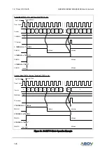


12. Timer 0/1/2/3/4/5
A96G140/A96G148/A96A148 User’s manual
138
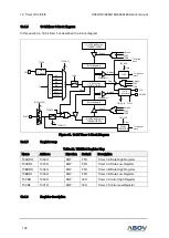
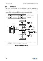
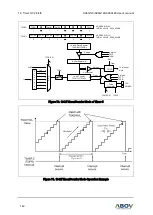
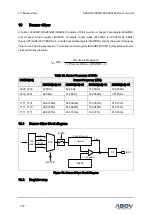
12.5.4
16-bit timer 4 block diagram
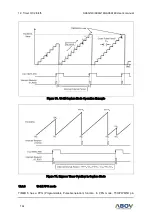
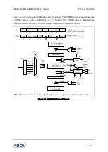
In this section, a 16-bit timer 4 is described in a block diagram.
T4MS[1:0]
T4POL
Reload
A Match
T4CC
T4EN
P
r
e
s
c
a
l
e
r
fx
M
U
X
fx/2
fx/4
fx/32
fx/128
fx/512
fx/8
fx/1
Comparator
16-bit Cou nte r
T4CNTH/T4CNTL
16-bit B Data Re gister
T4BDRH/T4BDRL
Clear
B Match
Buffer Reg ister B
Comparator
16-bit A Data Re gister
T4ADRH/T4ADRL
T4IFR
S/W
Clear
To i nte rrupt
block
A Match
Buffer Reg ister A
Reload
Pulse
Gen erator
T4O
R
EINT4
T4CNTR
T4EN
3
T4CK[2:0]
Clear
EIPOL0H[1:0]
FLAG4
(EIFLAG0.4)
INT_ACK
Clear
To i nte rrupt
block
2
2
T4MS[1:0]
2
T3 A Match
A Match
T4CC
T4EN
A Match
T4CC
T4EN
PWM4O
NOTE
: T3 A Match is a pulse for the timer 4 clock source if it is selected.
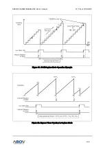
Figure 69. 16-bit Timer 4 Block Diagram
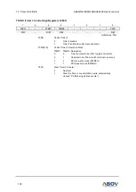
12.5.5
Register map
Table 23. TIMER 4 Register Map
Name
Address
Direction
Default
Description
T4ADRH
100AH
R/W
FFH
Timer 4 A Data High Register
T4ADRL
100BH
R/W
FFH
Timer 4 A Data Low Register
T4BDRH
100CH
R/W
FFH
Timer 4 B Data High Register
T4BDRL
100DH
R/W
FFH
Timer 4 B Data Low Register
T4CRH
1008H
R/W
00H
Timer 4 Control High Register
T4CRL
1009H
R/W
00H
Timer 4 Control Low Register
12.5.6
Register description