5-4
DECK MECHANISM DISASSEMBLY
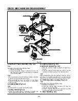
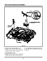
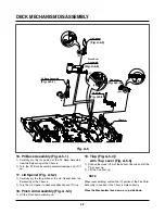
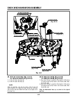
5. Up/Down Frame Assembly (Fig. 5-4)
Put the Main Base face down(Bottom Side)
1) Release the Screw(S4)
2) Unlock the Locking Tab(L3) in direction of arrow and
then lift up the Up/Down Frame Assembly to separate
it from the Base Main.
• When reassembling move the Up/Down Guide in direction
of arrow(C) until it is positioned as Fig.(C).
• When reassembling insert (A) portion of the Frame
Assembly Up/Down in the (B) portion of theUp/Down
Guide as Fig.(B)
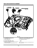
6. Loading Belt (Fig. 5-4)
Put the Base Main on original position(Top Side)
7. pulley Gear (Fig. 5-4)
1) Unlock the Locking Tab(L4) in direction of arrow(B) and
then separate the Pulley Gear from the Base Main.
8. Loading Gear (Fig. 5-4)
9. Up/Down Guide (Fig. 5-4)
1) Move the Up/Down Guide in direction of arrow(A) as
Fig.(A)
2) Push the Locking Tab(L5) down and then lift up the
Up/Down Guide to separate it from the Base Main.
When reassembling place the Up/Down Guide as Fig.(C)
and move it in direction arrow(B) until it is locked by the
Locking Tab(L5). And confirm the Up/Down Guide as Fig.(A)
10. PWB Assembly Loading (Fig. 5-4)
Put the Main Base face down(Bottom Side)
1) Release 2 Screws(S5)
2) Unkool the Loading Motor Connector (C2) from the
Hook (H1) on the Base Main.
3) Unlock 2 Locking Tabs(L6) and separate the PWB
Loading Assembly from the Base Main.
11. Base Main(Fig. 5-4)
Note
Note
Note
Note
Note
(L4)
(L6)
(L5)
(A)
(B)
(B)
(A)
(A)
(B)
(C)
(S5)
(C2)
(S4)
FIG. (A)
FIG. (C)
FIG. (B)
(H1)
(L6)
(L6)
(L3)
LOADING GEAR
PULLEY GEAR
PWB LOADING ASSEMBLY
LOADING BELT
MAIN BASE
UP/DOWN GUIDE
UP/DOWN GUIDE
UP/DOWN FRAME ASSEMBLY
MAIN BASE
UP/DOWN GUIDE
UP/DOWN GUIDE
Fig. 5-4
Содержание ABV341 Series
Страница 2: ......
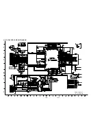
Страница 36: ...3 34 3 35 2 TU IF CIRCUIT DIAGRAM PB REC...
Страница 39: ...3 40 3 41 5 JACK CIRCUIT DIAGRAM...
Страница 41: ...3 44 3 45 7 TIMER CIRCUIT DIAGRAM XBV343...
Страница 42: ...3 46 3 47 8 TIMER CIRCUIT DIAGRAM XBV342...
Страница 45: ...3 52 3 53 PRINTED CIRCUIT DIAGRAMS 1 MAIN P C BOARD LOCATION GUIDE...
Страница 65: ...02 12 04 R17149A ZENITH DAP202K 3 80 3 81 6 JACK CIRCUIT DIAGRAM...
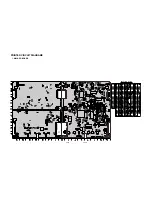
Страница 70: ...LOCATION GUIDE 3 90 3 91 PRINTED CIRCUIT DIAGRAMS 1 MAIN P C BOARD TOP VIEW...
Страница 71: ...LOCATION GUIDE 3 92 3 93 2 MAIN P C BOARD BOTTOM VIEW...
Страница 92: ...3 114 2 Audio related Signal ASDAT3 IC501 PIN 157 ABCK IC501 PIN 148 ALRCK IC501 PIN 149 ASDATA3 FIG 14 2...
Страница 98: ...3 121 3 122 2 RF DSP SERVO CIRCUIT DIAGRAM CD DVD LD will not on COMBI SCART MTK 03 3 25 SR17445A...
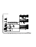
Страница 99: ...3 123 3 124 3 AUDIO CIRCUIT DIAGRAM COMBI SCART MTK 03 3 25 SR17447A...
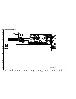
Страница 100: ...3 125 3 126 4 AV JACK CIRCUIT DIAGRAM COMBI SCART MTK 03 3 25 SR17446A...
Страница 103: ...3 131 3 132 PRINTED CIRCUIT DIAGRAMS 1 MAIN P C BOARD LOCATION GUIDE...
Страница 110: ...EXPLODED VIEW 1 Deck Mechanism Exploded View 5 1 CONTENTS SECTION 5 MECHANISM OF DVD PART MTK MODEL...
Страница 134: ...4 22 GEAR F R GEAR AY P2 P3 F R Lever Tension Base Boss CAM...

