


After the debug connections have been added to an Vivado IP integrator design, as shown
above, PCIe Link debug is enabled in the generated
.pdi
image. The connections shown above
should be added to a full design and are not sufficient to create a working design alone. The PCIe
IP ports and the remainder of the design must be created and configured as per the desired
operation of the PCIe-enabled IP.
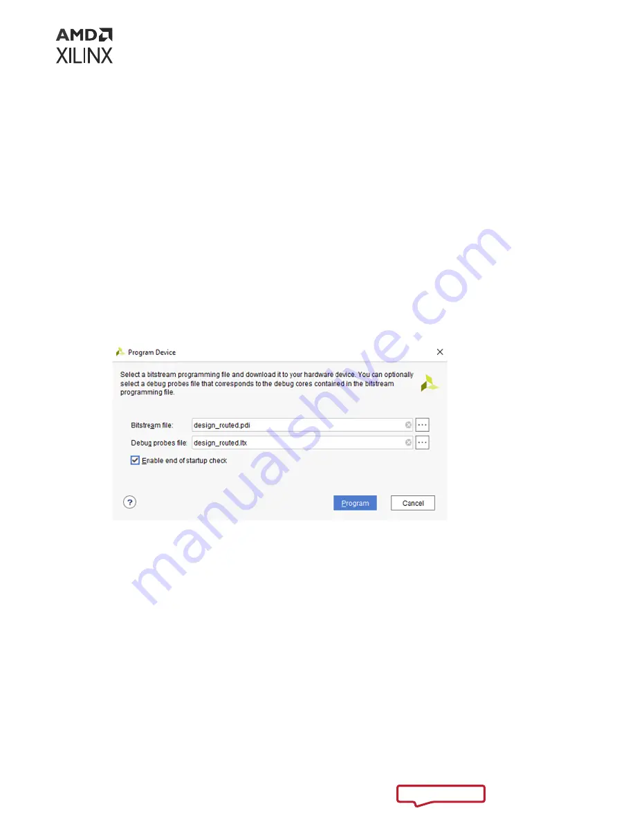
Connecting to PCIe Link Debug in Vivado
Use the following steps to connect Vivado Hardware Manager to the FPGA device and
associated PCIe Link Debug enabled design.
1. Open the Hardware Manager.
2. Select the device from the Tools → Program Device… drop-down menu.
3. Select the
.pdi
and
.ltx
files for programming the device, and select Program.
Note: You should not load the
.ltx
file and refresh the target until after the
.pdi
file has been
programmed.
4. Select the PCIe Debug core in the Hardware window. You will see three main views that
include the PCIe Debug Core Properties, PCIe Link LTSSM State Trace, and the PCIe Link
LTSSM State Diagram with transitions.
Appendix C: Debugging
PG346 (v3.3) November 16, 2022
CPM Mode for PCI Express
259


