


FPGA Registers
EPU-4562 Programmer’s Reference Manual
28
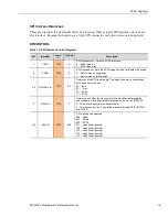
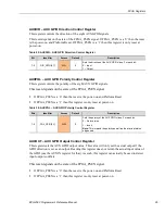
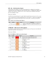
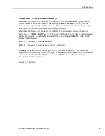
AUXMODE1– AUX I/O Mode Register #1
These two registers select the mode on each AUX GPIO.
This reset depends on the state of the FPGA_PSEN signal.
If FPGA_PSEN is a ‘0’ then the reset is the power-on and Platform Reset.
If FPGA_PSEN is a ‘1’ then this register is only reset at power-on.
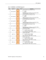
Table 35: AUXMODE1 – AUX I/O Mode Register
Bit
Identifier
Access
Default
Description
7
MODE_GPIO8
R/W
0
GPIO8 mode.
0 – GPIO (I/O)
1 – ICTC3 (input)
6
MODE_GPIO7
R/W
0
GPIO7 mode.
0 – GPIO (I/O)
1 – ICTC4 (input)
5
MODE_GPIO6
R/W
0
GPIO6 mode.
0 – GPIO (I/O)
1 – OCTC3 (output)
4
MODE_GPIO5
R/W
0
GPIO5 mode.
0 – GPIO (I/O)
1 – OCTC4 (output)
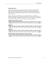
3
MODE_GPIO4
R/W
0
GPIO4 mode.
0 – GPIO (I/O)
1 – WDOG_RESET# (output only). In this mode, the GPIO will be
the FPGA watchdog timer trigger output that signals external
equipment that the watchdog fired.
The GPIO input status can still be read. Default is low-true.
Setting GPIO polarity to ‘1’ makes it high-true.
2
MODE_GPIO3
R/W
0
GPIO3 mode.
0 – GPIO (I/O)
1 – WAKE# (input only). In this mode, the GPIO is passed
through to the PCI_WAKE# signal.
Default is low-true. Setting GPIO polarity to ‘1’ makes it high-true.
The GPIO input status can still be read.
1
MODE_GPIO2
R/W
0
GPIO2 mode.
0 – GPIO (I/O)
1 – W_DISABLE# (input only). In this mode, the GPIO is passed
through to the W_DISABLE# signal.
The GPIO input status can still be read. Default is low-true.
Setting GPIO polarity to ‘1’ makes it high-true.
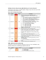
0
MODE_GPIO1
R/W
0
GPIO1 mode.
0 – GPIO (I/O)
1 – SLEEP# (input only). This is the sleep signal on the
baseboard power connector. It passes through the SLEEP# input
on the CPU module. Default is low-true. Setting GPIO polarity to
‘1’ makes it high-true.