


FPGA Registers
EPU-4562 Programmer’s Reference Manual
16
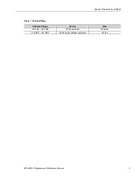
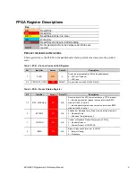
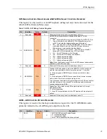
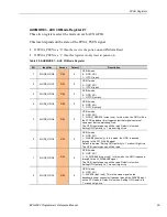
Bit
Identifier
Access
Default
Description
0
USB2_DIS1
R/W
0
Disable control for the paddleboard USB 2.0 ports 0,1 VBUS power
switches (there are two power-switches but they have a common power
enable and overcurrent status)
0 – VBUS power switches are enabled
1 – VBUS power switched are disabled.
Note:
The power switches latch-off in overcurrent and can only be re-
enabled by a power-cycle or by setting this bit to a ‘1’, wait >1msec and
then a ‘0’
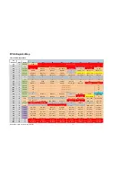
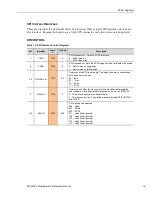
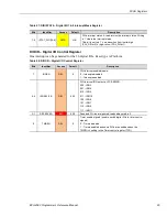
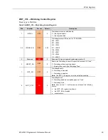
MISCSR3 – Miscellaneous Control Register #3
This register enables software to “push” the reset button.
Table 11: MISCSR3 – Misc. Control Register #3
Bits
Identifier
Access
Default
Description
7
PROCHOT
RO
N/A
The status of the THERMTRIP signal from the CPU module.
0 – THERMTRIP is not asserted (not hot)
1 – THERMTRIP is asserted
6
LVDS_OC
RO
N/A
The overcurrent status from the LVDS panel power switch. If this is
ever asserted, the LVDS panel enable signal must be de-asserted
and then asserted to “unlatch” the power fault condition on the
power switch.
0 – LVDS Overcurrent is not asserted
1 – LVDS Overcurrent is asserted
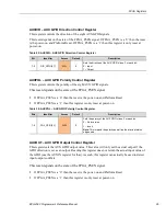
3-5
Reserved
RO
N/A
Reads the overcurrent status for the USB paddleboard power
switches (there are two power switches for the four ports but they
have a common overcurrent status).
0 – Overcurrent is not asserted (power switch is on)
1 – Overcurrent is asserted (power switch is off)
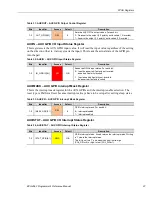
2
PBRESET
R/W
---
When written to, this will do the same thing as pushing the reset
button, which could be useful for a software-initiated watchdog.
0 – No action
1 – Activate the reset push-button
Note:
Because this generates a reset that will reset this register, it
isn’t likely a value of a ‘1’ can ever be read-back, so it is somewhat
“write-only”.
1-0
Reserved
RO
00
Reserved. Writes are ignored; reads always return 0.