


51
7
OPTION (Setting Code 38)
51
OP
TION
Chapter
7
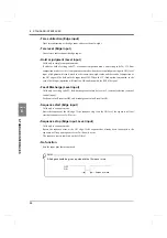
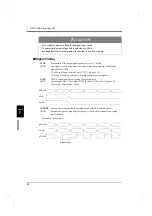
■
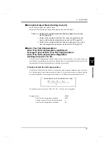
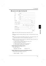
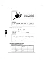
BCD Data Hold
Renewal of the BCD data output signal is stopped. Also the STROBE output is stopped. Switching
is done by A14.When COM and A14 are open: hold cancel, When they are short-circuited: hold on.
BCD data
OFF
ON
BCD data
1 cycle
1 cycle (max)
Renewal is stopped.
0
1
STROBE
hold
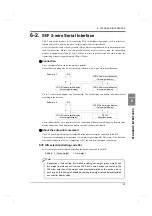
Read at least 2 cycles after inputting the BCD data hold.
As long as the BCD Data Hold signal is inputted, data can be read reliably, but because the data is
not renewed, it may be different from proper data.
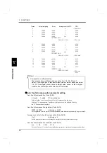
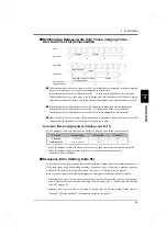
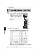
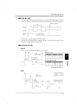
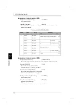
■
Equivalent Circuit
- Output
The signal output circuit is operated through an open collector.
COM
Vext
F160
Inside
Vceo=30V(max)
Ic=30mA(max)
●
Internal transistor status
Output data
Negative
Positive
0
OFF
ON
1
ON
OFF
●
Output pin level
Output data
Negative
Positive
0
H
L
1
L
H
Through logic switch (B14pin)
Outside
VCC
+5V
- Input
COM
+5V
TTL open collector output
(ON when IN is “ H”)
IN
IN
Approx.
Transistor
Open
OFF
Short
ON
Switch
F160
Inside Outside
Ic=6mA
Vcc
Содержание F160
Страница 1: ...01AUG2017REV 1 06 WEIGHING CONTROLLER F160 CC Link Ver 1 10 OPERATION MANUAL...
Страница 9: ...CONTENTS VIII CONTENTS VIII M E M O...
Страница 84: ...75 8 SPECIFICATIONS 75 SPECIFICATIONS Chapter 8 Equipped with BCD parallel data output interface option Unit mm...
Страница 85: ...76 8 SPECIFICATIONS 76 SPECIFICATIONS Chapter 8 Equipped with CC Link interface option Unit mm...
Страница 99: ......