


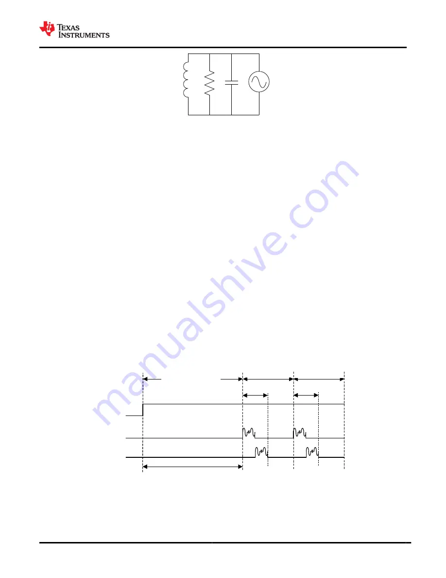
L
R
P
C
Figure 8-4. Equivalent Parallel Circuit
R
P
can be viewed as the load on the sensor driver. This load corresponds to the current drive required to
maintain the oscillation amplitude. R
P
must be between 350 Ω and 10 kΩ.
In summary, the LDC3114 requires that the sensor parameters are within the following ranges when the
conductive target is present:
• 1 MHz ≤
f
SENSOR
≤ 30 MHz
• 5 ≤ Q ≤ 30
• 350 Ω ≤ R
P
≤ 10 kΩ
8.1.3 Setting COM Pin Capacitor
The COM pin requires a bypass capacitor to ground. The capacitor should be a low-ESL, low-ESR type. C
COM
must be sized so that the following relationship is valid for all channels.
100 × C
SENSOR
n
/ Q
SENSOR
n
< C
COM
< 1250 × C
SENSOR
n
/ Q
SENSOR
n
(6)
The value of Q
SENSOR
n
when the sensor is at the minimum target distance should be used. The maximum
acceptable value for C
COM
is 20 nF. The C
COM
range for a particular sensor configuration can be obtained with
the Spiral_Inductor_Designer tab of the
.
8.1.4 Defining Power-On Timing
The low power architecture of the LDC3114 makes it possible for the device to be active all the time. When not
being used, the LDC3114 can operate in Low Power Mode with a single standby power button, which typically
consumes less than 10 µA. If additional power-saving is desired, or in the rare event where a power-on reset
becomes necessary (see
), the output data will become ready after 50-ms start-up time, about 1-ms
optional register loading time, and two sampling windows for all active channels.
shows the power-on
timing of the LDC3114.
VDD
IN0
66 ms startup time
25 ms scan cycle
Power up
DATA is ready
after all active channels
finish two conversions.
Only Channels 0 and 1 are enabled. Scan rate: 40 SPS.
Events
IN1
25 ms scan cycle
66 ms startup time is
independent of scan rate.
Sampling
Sampling
Figure 8-5. Power-On Timing
SNOSDD0 – DECEMBER 2021
Copyright © 2021 Texas Instruments Incorporated
39


