ST ST7LITEUS2 Скачать руководство пользователя страница 94

Obsolete Product(s) - Obsolete Product(s) 

Obsolete Product(s) - Obsolete Product(s) 

Electrical characteristics

ST7LITEUS2, ST7LITEUS5

94/136


12.3 Operating 

conditions

12.3.1 

General operating conditions

T

A

 = -40 to +125 °C unless otherwise specified.
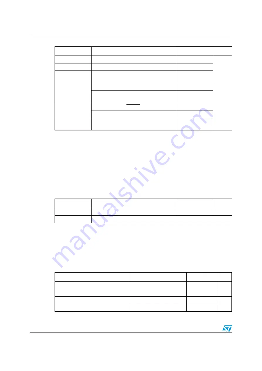
         

Table 44.

Current characteristics

Symbol

Ratings

 Maximum value

Unit

I

VDD

Total current into V

DD

 power lines (source)

(1)

1.

All power (V

DD

) and ground (V

SS

) lines must always be connected to the external supply.

75

mA

I

VSS

Total current out of V

SS

 ground lines (sink)

(1)

150

I

IO

Output current sunk by any standard I/O and 
control pin

20

Output current sunk by any high sink I/O pin

40

Output current source by any I/Os and control 
pin

-25

I

INJ(PIN)

 (2)(3)

2.

I

INJ(PIN)

 must never be exceeded. This is implicitly insured if V

IN

 maximum is respected. If V

IN

 maximum 

cannot be respected, the injection current must be limited externally to the I

INJ(PIN)

 value. A positive 

injection is induced by V

IN

>V

DD

 while a negative injection is induced by V

IN

<V

SS

.

3.

Negative injection disturbs the analog performance of the device. In particular, it induces leakage currents 
throughout the device including the analog inputs. To avoid undesirable effects on the analog functions, 
care must be taken:
- Analog input pins must have a negative injection less than 0.8 mA (assuming that the impedance of the 
analog voltage is lower than the specified limits)
- Pure digital pins must have a negative injection less than 1.6 mA. In addition, it is recommended to inject 
the current as far as possible from the analog input pins.

Injected current on RESET pin

± 5

Injected current on any other pin

(4)

4.

When several inputs are submitted to a current injection, the maximum 

Σ

I

INJ(PIN)

 is the absolute sum of the 

positive and negative injected currents (instantaneous values). These results are based on 
characterisation with 

Σ

I

INJ(PIN)

 maximum current injection on four I/O port pins of the device.

± 5

Σ

I

INJ(PIN)

(2)

Total injected current (sum of all I/O and control 
pins)

(4)

± 20

Table 45.

Thermal characteristics

Symbol

Ratings

 value

Unit

T

STG

Storage temperature range

-65 to +150

°C

T

J

Maximum junction temperature (see 

Section 13: Package characteristics

)

Table 46.

General operating conditions

Symbol

Parameter

 Conditions

Min

Max

Unit

V

DD

Supply voltage

f

CPU

 = 4 MHz max.

2.4

5.5

V

f

CPU 

= 8 MHz max.

3.3

5.5

f

CPU

CPU clock frequency

3.3 V

≤ 

V

DD

5.5 V

up to 8

MHz

2.4 V

V

DD

<

3.3 V

up to 4

      Obsolete Product(s) - Obsolete Product(s)

Содержание ST7LITEUS2

Страница 1: ...te timer LT with prescaler including watchdog one realtime base and one 8 bit input capture One 12 bit auto reload timer AT with output compare function and PWM A D Converter 10 bit resolution for 0 t...

Страница 2: ...ce 19 4 5 Memory protection 20 4 5 1 Readout protection 20 4 5 2 Flash Write Erase protection 21 4 6 Related documentation 21 4 7 Register description 22 4 7 1 Flash Control Status register FCSR 22 5...

Страница 3: ...ternal watchdog reset 37 6 5 Register description 37 6 5 1 Multiplexed I O Reset Control register 1 MUXCR1 37 6 5 2 Multiplexed I O Reset Control register 0 MUXCR0 37 7 Interrupts 39 7 1 Non maskable...

Страница 4: ...0 1 Lite timer LT 65 10 1 1 Introduction 65 10 1 2 Main features 65 10 1 3 Functional description 66 10 1 4 Low power modes 68 10 1 5 Interrupts 68 10 1 6 Register description 69 10 2 12 bit auto relo...

Страница 5: ...1 4 Loading capacitor 92 12 1 5 Pin input voltage 93 12 2 Absolute maximum ratings 93 12 3 Operating conditions 94 12 3 1 General operating conditions 94 12 3 2 Operating conditions with low voltage...

Страница 6: ...mechanical data 118 13 2 Thermal characteristics 122 14 Device configuration and ordering information 123 14 1 Option bytes 123 14 1 1 OPTION BYTE 1 123 14 1 2 OPTION BYTE 0 124 14 2 Ordering informat...

Страница 7: ...upt events 63 Table 22 Port configuration 64 Table 23 I O port register map and reset values 64 Table 24 Description of low power modes 68 Table 25 Interrupt events 68 Table 26 Lite timer register map...

Страница 8: ...64 Output driving current characteristics 109 Table 65 Asynchronous RESET pin characteristics 114 Table 66 10 bit ADC characteristics 115 Table 67 ADC accuracy with VDD 3 3 to 5 5 V 116 Table 68 ADC...

Страница 9: ...verview 53 Figure 24 Halt mode flowchart 53 Figure 25 AWUFH mode block diagram 54 Figure 26 AWUF Halt timing diagram 55 Figure 27 AWUFH mode flowchart 56 Figure 28 I O port general block diagram 61 Fi...

Страница 10: ...112 Figure 57 Typical VDD VOH at VDD 3 V HS pins 112 Figure 58 Typical VDD VOH at VDD 5 V HS pins 112 Figure 59 Typical VOL vs VDD HS pins 113 Figure 60 Typical VDD VOH vs VDD HS pins 113 Figure 61 R...

Страница 11: ...ng modes of the ST7 offer both power and flexibility to software developers enabling the design of highly efficient and compact application code In addition to standard 8 bit data management all ST7 m...

Страница 12: ...vector Figure 3 8 pin DFN package pinout 1 HS High sink capability 2 eix associated external interrupt vector VDD PA5 HS AIN4 CLKIN PA3 RESET VSS PA0 HS AIN0 ATPWM ICCDATA PA2 HS LTIC AIN2 PA1 HS AIN...

Страница 13: ...ns The RESET signal is mapped on a dedicated pin It is not multiplexed with PA3 PA3 pin is always configured as output Any change on multiplexed IO reset control registers MUXCR1 and MUXCR2 will have...

Страница 14: ...Input 3 PA4 AIN3 MCO I O CT HS X ei3 X X X Port A4 Analog input 3 or main clock output 4 PA3 RESET 1 O X X X Port A3 RESET 1 5 PA2 AIN2 LTIC I O CT HS X ei2 X X X Port A2 Analog input 2 or Lite Timer...

Страница 15: ...ng space so the reset and interrupt vectors are located in Sector 0 FE00h FFFFh The size of Flash Sector 0 and other device options are configurable by option byte Warning Memory locations marked as R...

Страница 16: ...rved area 3 bytes 0017h 0018h AUTO RELOAD TIMER DCR0H DCR0L PWM 0 Duty Cycle register High PWM 0 Duty Cycle register Low 00h 00h R W R W 0019h to 002Eh Reserved area 22 bytes 0002Fh FLASH FCSR Flash C...

Страница 17: ...eakpoint register 2 Low 00h 00h 00h 00h 00h 00h R W R W R W R W R W R W 0051h to 007Fh Reserved area 47 bytes 1 Legend x undefined R W read write 2 The contents of the I O port DR registers are readab...

Страница 18: ...ramming modes The ST7 can be programmed in three different ways Insertion in a programming tool In this mode FLASH sectors 0 and 1 and option byte row can be programmed or erased In circuit programmin...

Страница 19: ...in CLKIN main clock input for external source VDD application board power supply Refer to Figure 6 for a description of the I2 C interface If the ICCCLK or ICCDATA pins are only used as outputs in the...

Страница 20: ...a pull up is placed on PA3 for application reasons Caution During normal operation ICCCLK pin must be pulled up internally or externally external pull up of 10 k mandatory in noisy environment This i...

Страница 21: ...ed in the option list 4 5 2 Flash Write Erase protection Write erase protection when set makes it impossible to both overwrite and erase program memory Its purpose is to provide advanced security to a...

Страница 22: ...ing using ICP IAP or other programming methods 1st RASS Key 0101 0110 56h 2nd RASS Key 1010 1110 AEh When an EPB or another programming tool is used in socket or ICP mode the RASS keys are sent automa...

Страница 23: ...A The Accumulator is an 8 bit general purpose register used to hold operands and the results of the arithmetic and logic calculations and to manipulate data 5 3 2 Index registers X and Y In indexed a...

Страница 24: ...This register can also be handled by the PUSH and POP instructions These bits can be individually tested and or controlled by specific instructions Reset value 111x1xxx ACCUMULATOR X INDEX REGISTER Y...

Страница 25: ...I bit is cleared by software in the interrupt routine pending interrupts are serviced regardless of the priority level of the current interrupt routine Bit 2 N Negative This bit is set and cleared by...

Страница 26: ...limit is exceeded the Stack Pointer wraps around to the stack upper limit without indicating the stack overflow The previously stored information is then overwritten and therefore lost The stack also...

Страница 27: ...it 27 136 Figure 8 Stack manipulation example 1 Stack higher address 00FFh 2 Stack lower address 00C0h PCH PCL SP PCH PCL SP PCL PCH X A CC PCH PCL SP PCL PCH X A CC PCH PCL SP PCL PCH X A CC PCH PCL...

Страница 28: ...be calibrated to obtain the frequency required in the application This is done by software writing a 10 bit calibration value in the RCCR RC Control register and in the bits 6 5 in the SICSR SI Contr...

Страница 29: ...Section 14 1 on page 123 This is recommended for applications where very low power consumption is required Switching from one startup clock to another can be done in run mode as follows see Figure 9...

Страница 30: ...l set AWU RC 7 0 0 0 0 0 0 0 MCO SMS Read Write Bits 7 2 Reserved must be kept cleared Bit 1 MCO Main Clock Out enable bit This bit is read write by software and cleared by hardware after a reset This...

Страница 31: ...r each voltage range in Flash memory and write it to this register at startup 00h maximum available frequency FFh lowest available frequency Note To tune the oscillator write a series of different val...

Страница 32: ...cillator See Figure 10 on page 34 and Table 6 Bits 4 2 Reserved must be kept cleared Bits 1 0 AVD Threshold Selection bits Refer to Section 7 4 System integrity management SI Table 6 Internal RC presc...

Страница 33: ...pt cleared Bit 0 RC AWU RC AWU Selection 0 RC enabled 1 AWU enabled default value Table 7 Clock register map and reset values Address Hex Register label 7 6 5 4 3 2 1 0 0038h MCCSR Reset value 0 0 0 0...

Страница 34: ...s timebase 8 MHz fOSC fOSC 32 fOSC fOSC fLTIMER LITE TIMER COUNTER 13 BIT fCPU TO CPU AND 0 1 CR6 CR9 CR2 CR3 CR4 CR5 CR8 CR7 RCCR fOSC CLKIN Tunable Oscillator internal RC Option bits CKSEL 1 0 2 DIV...

Страница 35: ...vector is fixed at addresses FFFEh FFFFh in the ST7 memory map The basic reset sequence consists of 3 phases as shown in Figure 11 Active phase depending on the reset source 64 CPU clock cycle delay...

Страница 36: ...a major role in EMS performance In a noisy environment it is recommended to follow the guidelines mentioned in the electrical characteristics section 6 4 3 External Power on reset If the LVD is disabl...

Страница 37: ...nces 6 5 Register description 6 5 1 Multiplexed I O Reset Control register 1 MUXCR1 Reset value 0000 0000 00h 6 5 2 Multiplexed I O Reset Control register 0 MUXCR0 Reset value 0000 0000 00h VDD Run RE...

Страница 38: ...t the application program has to configure the I O port by writing to these registers as described above Once the pin is configured as an I O output it cannot be changed back to a reset pin by the app...

Страница 39: ...on of the interrupt service routine is fetched refer to the Interrupt Mapping table for vector addresses The interrupt service routine should finish with the IRET instruction which causes the contents...

Страница 40: ...the interrupt request even in case of rising edge sensitivity 7 3 Peripheral interrupts Different peripheral interrupt flags in the status register are able to cause an interrupt when they are active...

Страница 41: ...t PWMxCS R or ATCSR no FFEAh FFEBh 9 AT TIMER Overflow Interrupt ATCSR yes 3 FFE8h FFE9h 10 LITE TIMER LITE TIMER Input Capture Interrupt LTCSR no FFE6h FFE7h 11 LITE TIMER RTC1 Interrupt LTCSR yes 3...

Страница 42: ...sensitivity of a particular external interrupt clears this pending interrupt This can be used to clear unwanted pending interrupts Refer to Section External interrupt function 3 IS4 1 0 01 is the only...

Страница 43: ...vided the minimum VDD value guaranteed for the oscillator frequency is above VIT LVD the MCU can only be in two modes Under full software control In static safe reset In these conditions secure operat...

Страница 44: ...vs reset Figure 16 Reset and supply management block diagram VDD VIT LVD RESET VIT LVD Vhys LOW VOLTAGE DETECTOR LVD AUXILIARY VOLTAGE DETECTOR AVD RESET VSS VDD RESET SEQUENCE MANAGER RSM AVD Interru...

Страница 45: ...DTHCR register If the AVD interrupt is enabled an interrupt is generated when the voltage crosses the VIT AVD or VIT AVD threshold AVDF bit is set In the case of a drop in voltage the AVD interrupt ac...

Страница 46: ...exit from Wait mode Halt The SICSR register is frozen The AVD remains active but the AVD interrupt cannot be used to exit from Halt mode Table 12 Description of interrupt events Interrupt Event Event...

Страница 47: ...VD threshold during less than TAWU 33us typ the LVDRF flag cannot be set even if the device is reset by the LVD If the selected clock source is the external clock CLKIN the flag is never set if the re...

Страница 48: ...m Halt AWUFH Halt After a reset the normal operating mode is selected by default Run mode This mode drives the device CPU and embedded peripherals by means of a master clock which is based on the main...

Страница 49: ...vice is already in Slow mode Figure 19 Slow mode clock transition 8 3 Wait mode Wait mode places the MCU in a low power consumption mode by stopping the CPU This power saving mode is selected by calli...

Страница 50: ...tered by executing the HALT instruction The decision to enter either in Active halt or Halt mode is given by the LTCSR ATCSR register status as shown in the following table WFI INSTRUCTION RESET INTER...

Страница 51: ...the interrupt vector which woke it up see Figure 22 When entering Active halt mode the I bit in the CC register is cleared to enable interrupts Therefore if an interrupt is pending the MCU wakes up i...

Страница 52: ...is used to stabilize it After the start up delay the CPU resumes operation by servicing the interrupt or by fetching the reset vector which woke it up see Figure 24 When entering Halt mode the I bit i...

Страница 53: ...details 4 Before servicing an interrupt the CC register is pushed on the stack The I bit of the CC register is set during the interrupt routine and cleared when the CC register is popped 5 The CPU clo...

Страница 54: ...er executing the external interrupt routine corresponding to the wakeup event reset or external interrupt 8 5 Auto wakeup from Halt mode Auto wakeup from Halt AWUFH mode is similar to Halt mode with t...

Страница 55: ...The MCU can exit AWUFH mode by means of any interrupt with exit from Halt capability or a reset see Section 8 4 Active halt and Halt modes When entering AWUFH mode the I bit in the CC register is forc...

Страница 56: ...ls 4 Before servicing an interrupt the CC register is pushed on the stack The I 1 0 bits of the CC register are set to the current software priority level of the interrupt routine and recovered when t...

Страница 57: ...er This allows the timer to be used to measure the AWU RC oscillator dispersion and then compensate this dispersion by providing the right value in the AWUPRE register 0 Measurement disabled 1 Measure...

Страница 58: ...written to AWUPR depending on the product an interrupt is generated immediately after a HALT instruction or the AWUPR remains unchanged Table 15 Configuring the dividing factor AWUPR 7 0 Dividing fact...

Страница 59: ...not provide this register refer to the I O Port Implementation section The generic I O block diagram is shown in Figure 28 9 2 1 Input modes The input configuration is selected by clearing the corres...

Страница 60: ...external interrupt a Set the interrupt mask with the SIM instruction in cases where a pin level change could occur b Select rising edge c Enable the external interrupt through the OR register d Select...

Страница 61: ...n must be configured in floating input mode In this case the pin state is also digitally readable by addressing the DR register Note 1 Input pull up configuration can cause unexpected value at the inp...

Страница 62: ...e associated alternate function is enabled as an output reading the DR register will read the alternate function output status OPEN DRAIN OUTPUT 2 2 When the I O port is in output configuration and th...

Страница 63: ...close to a selected analog pin Warning The analog input voltage level must be within the limits stated in the absolute maximum ratings 9 3 Unused I O pins Unused I O pins must be connected to fixed v...

Страница 64: ...igure 29 Interrupt I O port state transitions The I O port register configurations are summarized in Table 22 After reset to configure PA3 as a general purpose output the application has to program th...

Страница 65: ...ture register and watchdog function 10 1 2 Main features Real time clock 13 bit upcounter 1 ms or 2 ms timebase period 8 MHz fOSC Maskable timebase interrupt Input capture 8 bit input capture register...

Страница 66: ...hdog reset occurring software must set the WDGD bit The WDGD bit is cleared by hardware after tWDG This means that software must write to the WDGD bit at regular intervals to prevent a watchdog reset...

Страница 67: ...llator When the oscillator is stopped the Lite Timer stops counting and is no longer able to generate a watchdog reset until the microcontroller receives an external interrupt or a reset If an externa...

Страница 68: ...tion Wait No effect on Lite timer Active Halt No effect on Lite timer Halt Lite timer stops counting Table 25 Interrupt events 1 1 The TBF and ICF interrupt events are connected to separate interrupt...

Страница 69: ...iting to this bit does not change the bit value 0 No input capture 1 An input capture has occurred Note After an MCU reset software must initialise the ICF bit by reading the LTICR register Bit 5 TB T...

Страница 70: ...Enable This bit is set and cleared by software 0 Watchdog disabled 1 Watchdog enabled Bit 0 WDGD Watchdog Reset Delay This bit is set by software It is cleared by hardware at the end of each tWDG peri...

Страница 71: ...cription PWM mode This mode allows a pulse width modulated signals to be generated on the PWM0 output pin with minimum core processing overhead The PWM0 output signal can be enabled or disabled using...

Страница 72: ...M0 signals is set to a low level To obtain a signal on the PWM0 pin the contents of the DCR0 register must be greater than the contents of the ATR register The polarity bit can be used to invert the o...

Страница 73: ...e function is only available for DCRx values other than 0 reset value Caution At each OVF event the DCRx value is written in a shadow register even if the DCR0L value has not yet been written in this...

Страница 74: ...K 1 0 Counter Clock Selection These bits are set and cleared by software and cleared by hardware after a reset They select the clock frequency of the counter see Table 29 Counter clock selection Bit 2...

Страница 75: ...is case CNTRH can be incremented between the two read operations and to have an accurate result when ftimer fCPU special care must be taken when CNTRL values close to FFh are read When a counter overf...

Страница 76: ...e is written by software The high register must be written first In PWM mode OE0 1 in the PWMCR register the DCR 11 0 bits define the duty cycle of the PWM0 output signal see Figure 34 In Output Compa...

Страница 77: ...eared by software by reading the PWM0CSR register It indicates that the upcounter value matches the DCR0 register value 0 Upcounter value does not match DCR value 1 Upcounter value matches DCR value 7...

Страница 78: ...0 ATR2 0 ATR1 0 ATR0 0 12 PWMCR Reset value 0 0 0 0 0 0 0 OE0 0 13 PWM0CSR Reset value 0 0 0 0 0 0 OP 0 CMPF0 0 17 DCR0H Reset value 0 0 0 0 DCR11 0 DCR10 0 DCR9 0 DCR8 0 18 DCR0L Reset value DCR7 0 D...

Страница 79: ...a 10 bit Data register The A D converter is controlled through a Control Status register 10 3 2 Main features 10 bit conversion Up to 5 channels with multiplexed input Linear successive approximation...

Страница 80: ...e conversion is stored in the ADCDRH and ADCDRL registers The accuracy of the conversion is described in the Electrical Characteristics Section RAIN is the maximum recommended impedance for an analog...

Страница 81: ...channel to convert ADC conversion mode In the ADCCSR register set the ADON bit to enable the A D converter and to start the conversion From this time on the ADC performs a continuous conversion of th...

Страница 82: ...tware reading the ADCDRH register 0 Conversion is not complete 1 Conversion complete Bit 6 SPEED ADC clock selection This bit is set and cleared by software It is used together with the SLOW bit to co...

Страница 83: ...by software It is used together with the SPEED bit to configure the ADC clock speed as shown on the table below see Table 33 Configuring the ADC clock speed Bit 2 Reserved Forced by hardware to 0 Bit...

Страница 84: ...ll memory to memory instructions use short addressing modes only CLR CPL NEG BSET BRES BTJT BTJF INC DEC RLC RRC SLL SRL SRA SWAP The ST7 Assembler optimizes the use of long and short addressing modes...

Страница 85: ...ction is executed the Program Counter PC points to the instruction following JRxx Table 36 ST7 addressing mode overview continued 1 Mode Syntax Destination source Pointer address Pointer size Length b...

Страница 86: ...ter the opcode 11 1 4 Indexed mode no offset short long In this mode the operand is referenced by its memory address which is defined by the unsigned addition of an index register X or Y with an offse...

Страница 87: ...nd is referenced by its memory address which is defined by the unsigned addition of an index register value X or Y with a pointer value located in memory The pointer address follows the opcode The ind...

Страница 88: ...lustrated in the following table CPL NEG 1 or 2 complement BSET BRES Bit operations BTJT BTJF Bit test and jump operations SLL SRL SRA RLC RRC Shift and rotate operations SWAP Swap nibbles CALL JP Cal...

Страница 89: ...essing mode It also changes an instruction using X indexed addressing mode to an instruction using indirect X indexed addressing mode PIY 91 Replace an instruction using X indirect indexed addressing...

Страница 90: ...Increment inc X reg M N Z JP Absolute jump jp TBL w JRA Jump relative always JRT Jump relative JRF Never jump jrf JRIH Jump if ext interrupt 1 JRIL Jump if ext interrupt 0 JRH Jump if H 1 H 1 JRNH Jum...

Страница 91: ...reg M N Z C RSP Reset Stack Pointer S Max allowed SBC Subtract with carry A A M C A M N Z C SCF Set carry flag C 1 1 SIM Disable interrupts I 1 1 SLA Shift left arithmetic C Dst 0 reg M N Z C SLL Shif...

Страница 92: ...haracteristics are indicated in the table footnotes and are not tested in production Based on characterization the minimum and maximum values refer to sample tests and represent the mean value plus or...

Страница 93: ...occurs for example due to a corrupted program counter To guarantee safe operation this connection has to be done through a pull up or pull down resistor typical 10 k for I Os Unused I O pins must be...

Страница 94: ...device including the analog inputs To avoid undesirable effects on the analog functions care must be taken Analog input pins must have a negative injection less than 0 8 mA assuming that the impedance...

Страница 95: ...eshold Low threshold 3 9 3 2 2 5 4 2 3 5 2 7 4 5 3 8 3 0 V VIT LVD Reset generation threshold VDD fall High threshold Med threshold Low threshold 3 7 3 0 2 4 4 0 3 3 2 6 4 3 3 6 2 9 Vhys LVD voltage t...

Страница 96: ...haracterization Typ 2 Max 2 Unit VIT AVD 1 0 AVDF flag toggle threshold VDD rise High threshold Med threshold Low threshold 4 0 3 4 2 6 4 4 3 7 2 9 4 8 4 1 3 2 V VIT AVD 0 1 AVDF flag toggle threshold...

Страница 97: ...VDD 4 5 to 5 5 V 2 3 0 5 0 TA 40 C to 0 C VDD 4 5 to 5 5 V 2 4 0 2 5 tsu RC RC oscillator setup time TA 25 C VDD 5 V 4 2 s 1 See Section 6 2 Internal RC oscillator adjustment 2 Tested in production a...

Страница 98: ...vs VDD 2 4 6 0V and temperature 2 2 2 0 1 8 1 6 1 4 1 2 1 0 0 8 0 6 0 4 0 2 0 0 0 2 0 4 0 6 0 8 1 0 1 2 1 4 1 6 1 8 2 0 2 2 2 4 2 8 3 2 3 6 4 0 4 4 4 8 5 2 5 6 6 0 Accuracy RC5V 45C RC5V 25C RC5V 90C...

Страница 99: ...300 400 2 A Supply current in Slow wait mode 5 fCPU 32 250 kHz 250 350 2 Supply current in AWUFH mode 6 7 20 50 2 Supply current in Active halt mode 90 150 2 Supply current in Halt mode 8 TA 85 C 0 25...

Страница 100: ...int RC 4 MHz 1 0 1 6 TA 25 C int RC 2 MHz 0 9 1 5 Supply current in Slow mode 4 TA 25 C int RC 32 250 kHz 0 95 1 5 Supply current in Slow Wait mode 5 TA 25 C int RC 32 250 kHz 0 85 1 4 Supply current...

Страница 101: ...ctive halt mode vs VDD int RC 8 MHz IddRUNm ode am bvsintclockfreq 0 00 1 00 2 00 3 00 4 00 5 00 6 00 2 4 2 6 2 8 3 3 2 3 4 3 6 3 8 4 4 2 4 4 4 6 4 8 5 5 2 5 4 5 6 VDD V Idd RUN mA RC8M Hz RC4M Hz RC2...

Страница 102: ...VDD 5 V int RC 8 MHz Figure 46 IDD vs temp VDD 5 V int RC 4 MHz Figure 47 IDD vs temp VDD 5 V int RC 2 MHz 0 0 1 0 2 0 3 0 4 0 5 0 6 0 45 25 90 130 Temp C Idd mA run wfi slow slowwait acthlt 0 0 0 5 1...

Страница 103: ...sed on a differential IDD measurement between reset configuration and continuous A D conversions with amplifier off Table 55 General timings Symbol Parameter 1 1 Data based on characterization Not tes...

Страница 104: ...et or in hardware registers only in Halt mode Guaranteed by construction not tested in production 5 5 V tprog Programming time for 1 32 bytes 2 2 Up to 32 bytes can be programmed at a time TA 40 to 12...

Страница 105: ...ified MCU software It should be noted that good EMC performance is highly dependent on the user application and the software in particular Therefore it is recommended that the user applies EMC softwar...

Страница 106: ...Body Model This test conforms to the JESD22 A114A A115A standard Static and dynamic latchup LU 3 complementary static tests are required on 10 parts to assess the latchup performance A supply overvol...

Страница 107: ...J1752 3 standards For more details refer to the application note AN1181 Table 62 Electrical sensitivities Symbol Parameter Conditions Class 1 1 Class description A Class is an STMicroelectronics inter...

Страница 108: ...S VIN VDD 1 A IS Static current consumption induced by each floating input pin 2 2 Configuration not recommended all unused pins must be kept at a fixed voltage using the output mode of the I O for ex...

Страница 109: ...Figure 51 V DD 3 V IIO 2 mA TA 125 C 500 Output low level voltage for a high sink I O pin when 4 pins are sunk at same time see Figure 54 IIO 2 mA TA 125 C 180 IIO 8 mA TA 125 C 600 VOH 2 3 Output hi...

Страница 110: ...andard pins Figure 51 Typical VOL at VDD 3 V standard pins Figure 52 Typical VOL at VDD 5 V standard pins 0 200 400 600 800 1000 1200 1400 0 2 4 Iol mA VOL mV 45 C 25 C 90 C 130 C 0 200 400 600 800 10...

Страница 111: ...ypical VOL at VDD 3 V HS pins Figure 55 Typical VOL at VDD 5 V HS pins 0 200 400 600 800 1000 1200 0 2 4 6 8 10 12 14 16 Iol mA VOL mV 45 C 25 C 90 C 130 C 0 200 400 600 800 1000 1200 1400 0 2 4 6 8 1...

Страница 112: ...D 3 V HS pins Figure 58 Typical VDD VOH at VDD 5 V HS pins 0 200 400 600 800 1000 1200 1400 1600 1800 0 2 4 6 8 10 12 Iol mA VDD VOH mV 45 C 25 C 90 C 130 C 0 200 400 600 800 1000 1200 1400 1600 1800...

Страница 113: ...hat the current sunk on the RESET pin is less than the absolute maximum value specified for IINJ RESET in Table 44 Refer to Figure 61 and Figure 62 for a description of the RESET pin protection circui...

Страница 114: ...ge induced by the capacitive effect of the power supply this will add 5 A to the power consumption of the MCU Table 65 Asynchronous RESET pin characteristics 1 1 TA 40 C to 125 C unless otherwise spec...

Страница 115: ...allowed within VDD 2 4 to 2 7 V operating range is 1 MHz 4 MHz VAIN Conversion voltage range 3 3 When VDDA and VSSA pins are not available on the pinout the ADC refers to VDD and VSS VSSA VDDA V RAIN...

Страница 116: ...3 V Symbol 1 1 Data based on characterization results over the whole temperature range Parameter Conditions Typ Max Unit ET Total unadjusted error fCPU 4 MHz fADC 2 MHz 1 2 0 3 0 LSB EO Offset error 0...

Страница 117: ...et Error deviation between the first actual transition and the first ideal one 6 EG Gain Error deviation between the last ideal transition and the last actual one 7 ED Differential Linearity Error max...

Страница 118: ...thin fine pitch dual flat no lead package outline Table 70 8 lead very thin fine pitch dual flat no lead package mechanical data Dim mm inches 1 1 Values in inches are converted from mm and rounded to...

Страница 119: ...ata Dim mm inches 1 1 Values in inches are converted from mm and rounded to 4 decimal digits Min Typ Max Min Typ Max A 1 35 1 75 0 0530 0 0690 A1 0 10 0 25 0 0040 0 0100 A2 1 10 1 65 0 0430 0 0650 B 0...

Страница 120: ...decimal digits Min Typ Max Min Typ Max A 5 33 0 2100 A1 0 38 0 0150 A2 2 92 3 30 4 95 0 1150 0 1300 0 1950 b 0 36 0 46 0 56 0 0140 0 0180 0 0220 b2 1 14 1 52 1 78 0 0450 0 0600 0 0700 b3 0 76 0 99 1 1...

Страница 121: ...ounded to 4 decimal digits Min Typ Max Min Typ Max A 5 33 0 2100 A1 0 38 0 0150 A2 2 92 3 30 4 95 0 1150 0 1300 0 1950 b 0 36 0 46 0 56 0 0140 0 0180 0 0220 b2 1 14 1 52 1 78 0 0450 0 0600 0 0700 c 0...

Страница 122: ...m junction temperature 1 1 The maximum chip junction temperature is based on technology characteristics 150 C PDmax Power dissipation 2 2 The maximum power dissipation is obtained from the formula PD...

Страница 123: ...The two option bytes allow the hardware configuration of the microcontroller to be selected The option bytes can be accessed only in programming mode for example using a standard ST7 programming tool...

Страница 124: ...e following table see Table 77 Definition of sector 0 size Bit 1 FMP_R Readout protection Readout protection when selected provides a protection against program memory content extraction and against w...

Страница 125: ...ill be pleased to provide detailed information on contractual points Table 78 OPTION BYTE 0 7 0 OPTION BYTE 1 7 0 Reserved SEC0 FMPR FMPW CKSEL 1 CKSEL 0 Res Res LVD1 LVD0 WDG SW WDG HALT Default valu...

Страница 126: ...bit SO8 Tube ST7PLUSA5M3TR 10 bit SO8 Tape Reel ST7PLUSA5U3 10 bit DFN8 Tray ST7PLUSA5U3TR 10 bit DFN8 Tape Reel ST7PLUSA2B3 1 Kbyte FASTROM 128 40 C 125 C DIP8 Tube ST7PLUSA2M3 SO8 Tube ST7PLUSA2M3T...

Страница 127: ...ng No Yes _ _ _ _ _ _ _ _ Authorized characters are letters digits and spaces only Maximum character count PDIP8 SO8 DFN8 8 char max _ _ _ _ _ _ _ _ Temperature range 40 C to 85 C 40 C to 125 C Clock...

Страница 128: ...U3 series emulators cost effective ST7 DVP3 series emulators and the low cost RLink in circuit debugger programmer These tools are supported by the ST7 Toolset from STMicroelectronics which includes t...

Страница 129: ...ble 81 ST7 application notes Identification Description Application examples AN1658 Serial numbering implementation AN1720 Managing the readout protection in flash microcontrollers AN1755 A high resol...

Страница 130: ...mplement a USB game pad AN1276 BLDC motor start routine for the ST72141 microcontroller AN1321 Using the ST72141 motor control MCU in sensor mode AN1325 Using the ST7 USB low speed firmware V4 x AN144...

Страница 131: ...ng microcontroller EMC performance AN1040 Monitoring the Vbus signal for USB Self powered devices AN1070 ST7 checksum self checking capability AN1181 Electrostatic Discharge sensitive measurement AN13...

Страница 132: ...rivers for ST7 HDFLASH or XFLASH MCUs AN1577 Device firmware upgrade DFU implementation for ST7 USB applications AN1601 Software implementation for ST7DALI EVAL AN1603 Using the ST7 USB device firmwar...

Страница 133: ...S5 Known limitations 133 136 15 Known limitations External interrupt 2 ei2 Whatever the external interrupt sensitivity configured through EICR1 register ei2 cannot exit the MCU from Halt Active halt a...

Страница 134: ...eup from Halt mode Replaced bit 1 by bit 2 for AWUF bit in Section 8 5 1 Register description Modified Section 9 1 Introduction Modified Section External interrupt function Updated Section 9 5 Interru...

Страница 135: ...ter 2 EICR2 Added Figure 41 and Figure 40 Added a note to LVDRF in Section 7 4 4 Register description Section 6 4 1 Introduction Modified Table 47 and Table 48 Modified Table 50Updated Table 53 Update...

Страница 136: ...OUT LIMITATION IMPLIED WARRANTIES OF MERCHANTABILITY FITNESS FOR A PARTICULAR PURPOSE AND THEIR EQUIVALENTS UNDER THE LAWS OF ANY JURISDICTION OR INFRINGEMENT OF ANY PATENT COPYRIGHT OR OTHER INTELLEC...

Отзывы: