58
6-1. IC AND FLUORESCENT DISPLAY TUBE CHECK
(SELF-DIAGNOSIS)
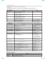
The communication between microcomputer and main ICs (self-
diagnosis) and the fluorescent display tube all lit are checked.
Checking Method:
1. After setting the test mode, rotate the
[ AMS ]
dial to
select “92. SET CHECK” and press the
[ AMS ]
dial
to enter.
2. When “SET TEST START” is displayed, rotate the
[ AMS ]
dial clockwise by 1 click to select “0. IC&FL
CHECK?” and press the
[ AMS ]
dial to enter.
3. A checking will start automatically, and “0. IC&FL CHECK”
will be displayed. (Checking time is about 3 seconds)
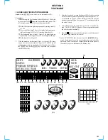
4. After IC communication check, all segments of fluorescent
display tube will be lit. At this time, check visually for a skipped
character.
5. At successful completion of check, “0. IC CHECK OK” is
displayed. In this case, no error exists in the IC interface. Pro-
ceed to 6-2. AUTO CHECK.
Note:
The check mentioned above tests the communication from micro-
computer to main ICs. Even if the check successfully finished, the
IC to be checked is not always normal. Consider it for reference
only.
6. In case of an IC communication error, the following display
will be given during the checking. Possible causes of error are
as listed below.
Error display
Causes (typical example)
DVD DEC. ERROR
1. IC701 (SACD decoder) is faulty
2. IC701 pin
<znv
(XRST) does not go “H”
• IC901 pin
rf
(XDIS) does not go “H”
• IC902 (expander) is faulty
3. 768fs (33.86688 MHz) is not present to
IC701 pin
<znm
(XTAL)
• IC811 (3-multiplying circuit) is faulty
• Clock signal 256fs is not sent from
AUDIO board (CN901 pin
qg
)
• CN901 pin
qh
(DFGND) and pin
qf
(DF3V) are open or shorted
• CN901 pin
qh
(DFGND) and pin
qf
(DF3V) are open or shorted
• CN901 and FFC connection is loose,
or FFC is disconnected
DVD DRAM ERR
1. IC706 (D-RAM) is faulty
2. IC701 pin
<znv
(XRST) does not go “H”
• IC901 pin
rf
(XDIS) does not go “H”
• IC902 (expander) is faulty
3. Faulty communication line between
IC701 and IC706
• Data line, address line, WE, etc.
4. D903 (1SS367) is faulty
CD DSP ERROR
1. IC509 (CD DSP) is faulty
2. 768fs (33.86688 MHz) is not present to
IC509 pin
ua
(XTAL)
Same as cause 3 of DVD DEC. ERROR
3. IC509 pin
2
(XRST) does not go “H”
• IC901 pin
rf
(XDIS) does not go “H”
• IC902 (expander) is faulty
D/A ERROR
1. IC904 (D/A converter) is faulty
2. Faulty IC703 (jitter amplifier) peripheral
circuits
3. IC901 pin
yf
(JIT) is faulty
EEPROM ERROR
1. IC903 (EEPROM) is faulty
Error display
Causes (typical example)
PRAWN DRAM ERR
1. IC808 (D-RAM) is faulty
*1
2. IC801 (DSD decoder) is faulty
3. 768fs (33.86688 MHz) is not present to
IC801 pin
qf
(MCKI)
Same as cause 3 of DVD DEC. ERROR
4. IC801 pin
qd
(XRST) does not go “H”
• IC901 pin
rf
(XDIS) does not go “H”
• IC902 (expander) is faulty
5. Faulty communication line between
IC801 and IC808
• Data line, address line, WE, etc.
6. D903 (1SS367) is faulty
D+3.3V is not present to IC808
RF AMP ERROR
1. IC001 (RF AMP) is faulty
2. Loose connection between CN503 on
MAIN board and CN001 on RF board,
or FFC disconnection
CN503 pin
ql
(CLK RF), pin
w;
(DATA
RF) and pin
wa
(SDEN) must be checked
SRAM ERROR
1. IC908 (SRAM) is defective.
2. IC907, IC909 (address conversion IC) are
defective.
3. The power voltage (3.3 V) is not supplied
to IC908.
C963 (Dual layer capacitor for backup) is
defective.
Q905 is defective.
4. IC908 pin-20 (XCE) does not go low.
Q901 (digital transistor) is defective.
D902 is defective.
*1 DSD decoder is also checked.
Causes Common to Each IC:
1. Faulty communication line between microcomputer and each
IC.
Disconnected patterns, floating series resistors, bridge, etc.
2. Faulty IC supply voltage.
Particularly, check D+3.3V voltage. (D+5V for display mi-
crocomputer)
3. The power supply voltage for the IC is 3.3V that is generated
by dividing the D5V using the voltage dividing with resistor
network and transistor for SRAM (IC908).
4. Faulty microcomputer communication port to each IC
Note:
In case of more than two errors, the error display is switched over
one after another, thus making the reading difficult.
In such a case, press again the
[ AMS ]
dial to make a
recheck for error reading.
l
L
l
L
l
L
l
L
l
L
Содержание SCD-C333ES - Super Audio Cd Changer
Страница 18: ...SCD C333ES 18 18 4 2 SCHEMATIC DIAGRAM RF SECTION Refer to page 40 for Waveforms ...
Страница 22: ...SCD C333ES 22 22 4 6 SCHEMATIC DIAGRAM MAIN SECTION 1 5 Refer to page 49 for IC Pin Function PIN FUNCTION ...
Страница 28: ...SCD C333ES 28 28 4 12 SCHEMATIC DIAGRAM AUDIO SECTION 2 3 ...
Страница 29: ...SCD C333ES 29 29 4 13 SCHEMATIC DIAGRAM AUDIO SECTION 3 3 ...
Страница 31: ...SCD C333ES 31 31 4 15 PRINTED WIRING BOARD AUDIO SECTION SIDE B Refer to page 12 for Circuit Board Location ...
Страница 32: ...SCD C333ES 32 32 4 16 SCHEMATIC DIAGRAM DISPLAY SECTION Refer to page 45 for IC Block Diagrams ...
Страница 34: ...SCD C333ES 34 34 4 18 SCHEMATIC DIAGRAM HP SECTION ...
Страница 36: ...SCD C333ES 36 36 4 20 SCHEMATIC DIAGRAM SENSOR SECTION Refer to page 45 for IC Block Diagram ...
Страница 38: ...SCD C333ES 38 38 4 22 SCHEMATIC DIAGRAM POWER SECTION ...


