50
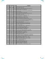
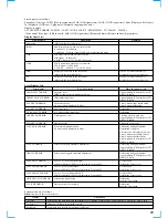
Pin No.
61
62, 63
64
65
66 to 69
70
71
72
73 to 75
76
77
78
79, 80
81
82 to 87
88
89
90
91
92
93
94
95
96, 97
98
99
100
101, 102
103
104 to 106
107
108
109
110
111
112
113, 114
115
116
117
118, 119
120
121
122, 123
124
125
126, 127
128, 129
130
131
Pin Name
VSS
HCS0, HCS1
VDD
DASP
MDB0 to MDB3
VSS
MDB4
VDD5V
MDB5 to MDB7
XMWR
VDD
XRAS
MA0, MA1
VSS
MA2 to MA7
VDD
MA8
VSS
MA9/MNT0
MA10/MNT1
MA11/MNT2
XMOE
XCAS
MDB8, MDB9
VSS
MDBA
VDD
MDBB, MDBC
VDD5V
MDBD to MDBF
GFS
VSS
APEO
VDD
DASYO
GNDA5
ASF1, AFS2
DASYI
RFDCC
RF IN
VCCA5, VCCA4
VCOR1
VCOIN
GNDA4, GNDA3
LPF5
VC1
LPF2, LPF1
VCCA3, VCCA2
PDO
PDHVCC
I/O
—
I
—
I/O
I/O
—
I/O
—
I/O
O
—
O
O
—
O
—
O
—
O
O
O
O
O
I/O
—
I/O
—
I/O
—
I/O
O
—
O
—
O
—
—
I
I
I
—
—
I
—
O
I
I
—
O
I
Description
Ground terminal (digital system)
Not used (open)
Power supply terminal (+3.3V) (digital system)
Not used (pull up)
Two-way data bus with the D-RAM (IC706)
Ground terminal (digital system)
Two-way data bus with the D-RAM (IC706)
Power supply terminal (+5V)
Two-way data bus with the D-RAM (IC706)
Write enable signal output to the D-RAM (IC706)
Power supply terminal (+3.3V) (digital system)
Row address strobe signal output to the D-RAM (IC706)
Address signal output to the D-RAM (IC706)
Ground terminal (digital system)
Address signal output to the D-RAM (IC706)
Power supply terminal (+3.3V) (digital system)
Address signal output to the D-RAM (IC706)
Ground terminal (digital system)
Address signal output to the D-RAM (IC706)
RF data signal output terminal for disc mark detection
Clock signal output terminal for disc mark detection
Monitor signal output to the CPU (IC901)
Output enable signal output to the D-RAM (IC706)
Column address strobe signal output to the D-RAM (IC706)
Two-way data bus with the D-RAM (IC706)
Ground terminal (digital system)
Two-way data bus with the D-RAM (IC706)
Power supply terminal (+3.3V) (digital system)
Two-way data bus with the D-RAM (IC706)
Power supply terminal (+5V)
Two-way data bus with the D-RAM (IC706)
Guard frame sync signal output to the CPU (IC901)
Ground terminal (digital system)
Absolute phase error signal output
Power supply terminal (+3.3V) (digital system)
RF binary signal output
Ground terminal (analog system)
Filter connected terminal for selection the constant asymmetry compensation
Analog signal input after integrated from the RF binary signal
Input terminal for adjusting DC cut high-pass filter for RF signal
RF signal input from the CXD1881R (IC001)
Power supply terminal (+3.3V) (analog system)
VCO oscillating range setting resistor connected terminal
VCO input terminal
Ground terminal (analog system)
Signal output from the operation amplifier from PLL loop filter
Middle point voltage (+1.65V) input terminal
Inverted signal input to the operation amplifier from PLL loop filter
Power supply terminal (+3.3V) (analog system)
Signal output from the charge pump for phase comparator
Middle point voltage input terminal for RF PLL
Содержание SCD-C333ES - Super Audio Cd Changer
Страница 18: ...SCD C333ES 18 18 4 2 SCHEMATIC DIAGRAM RF SECTION Refer to page 40 for Waveforms ...
Страница 22: ...SCD C333ES 22 22 4 6 SCHEMATIC DIAGRAM MAIN SECTION 1 5 Refer to page 49 for IC Pin Function PIN FUNCTION ...
Страница 28: ...SCD C333ES 28 28 4 12 SCHEMATIC DIAGRAM AUDIO SECTION 2 3 ...
Страница 29: ...SCD C333ES 29 29 4 13 SCHEMATIC DIAGRAM AUDIO SECTION 3 3 ...
Страница 31: ...SCD C333ES 31 31 4 15 PRINTED WIRING BOARD AUDIO SECTION SIDE B Refer to page 12 for Circuit Board Location ...
Страница 32: ...SCD C333ES 32 32 4 16 SCHEMATIC DIAGRAM DISPLAY SECTION Refer to page 45 for IC Block Diagrams ...
Страница 34: ...SCD C333ES 34 34 4 18 SCHEMATIC DIAGRAM HP SECTION ...
Страница 36: ...SCD C333ES 36 36 4 20 SCHEMATIC DIAGRAM SENSOR SECTION Refer to page 45 for IC Block Diagram ...
Страница 38: ...SCD C333ES 38 38 4 22 SCHEMATIC DIAGRAM POWER SECTION ...

