60
Items
Description
Remarks
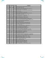
HENSIN
Eccentricity measurement
For the CD only are measured
Eccentricity (actual eccentric amount) of disc, disc pulley total
• Read by dividing by 10
• 0 may be displayed if eccentricity
is small (10um or less) (Due to
measurement reason)
SPIN DOWN TIME (msec)
Time from spindle brake application to rotation stop
For CD: Over 64 monitoring
For SACD: VCO1D monitoring
LOAD OUT TIME (msec)
Time until loading table comes out from the state where a disc is in chuck
Loading out switch H
t
L
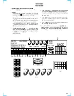
Measured Data Reading Method:
To judge the check result, the measured data must be read.
1. When “AUTO CHECK OK” is displayed, rotate the
[ AMS ]
dial clockwise by 2 clicks.
2. When “13. DISP RSLT?” is displayed, press the
[ AMS ]
dial to enter.
3. “PLEASE WAIT” will be displayed and in several seconds, “13. DISP RESULT” will be displayed.
4. Rotate the
[ AMS ]
dial clockwise by 1 click, and the “LOAD IN” will be displayed.
5. Press the
[ AMS ]
dial to enter. The LOAD IN TIME measured value will be displayed.
6. Compare the displayed value with the following specified value.
7. Hence, repeat step 4 to 6 (display is variable) and read the measured data respectively.
8. Compare the measured data with the specified value to check for NG item.
Note:
Blank display of measured value means that an error occurred during the checking or no measurement was taken place.
Specified Value:
(1) SACD (Use the test disc SATD-S4)
Note:
Measured values in check items are typical ones.
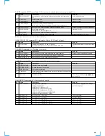
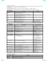
Check items
Specified value
LOAD IN TIME (msec)
:
Not displayed in this set.
SPIN UP TIME (msec)
: 1652
2000 msec or less
RF/VC/FE/TE AVRG (ORG)
: 98, C, 1DE, 0
RF: 80-9B, VC: 1F1-10, FE: 1d8-42, TE: 1BB-5C
RF/VC/FE/TE AVRG (ADJ)
: 9F, C, 4, 0
RF: 98-A5, VC : 1F1-10, FE: 1F1-10, TE: 1F1-10
PI/TRVS PP (ORG/ADJ)
: 81, 131, 78, 105
PI ORG: 70-8A, PI ADJ: 122-135
PIOR/CCR/TRCR
: 1A, 31, 1F
No specified value given
FOCUS/TRK GAIN
: 2E, 24
FOCUS: 1C-45, TRK: 1C-45
FBIAS/TRVSC/TRCR2/CFR
: 2,13, 6, 60
F.BIAS: 1D0-4F, TRVSC: 1D0-35 TRCR2, CFR: no specified value given
READ TOC TIME (msec)
: 1283
2500 msec or less
PSP AMPLITUDE
: 1666
1200 msec or above
1/3 SEEK TIME
F) AVE/MIN/MAX (msec)
: 967, 928, 990
AVE: 1200 msec or less, MAX: 1500 msec or less
R) AVE/MIN/MAX (msec)
: 974, 933, 993
AVE: 1200 msec or less, MAX: 1500 msec or less
1/MAX SEEK TIME
F) AVE/MIN/MAX (msec)
: 1958, 1938, 1968
AVE: 2500 msec or less, MAX: 3000 msec or less
R) AVE/MIN/MAX (msec)
: 1915, 1909, 1935
AVE: 2500 msec or less, MAX: 3000 msec or less
ERROR RATE
PO MAX/AVE FRAME
: 0, 0
No specified value given
PO MAX/AVE NUM
: 160, 3
MAX: 1000 msec or less, AVE: 200 msec or less
PI1 MAX/AVE FRAME
: 0, 0
No specified value given
PI1 MAX/AVE NUM
: 242, 17
MAX: 1000 msec or less, AVE: 200 msec or less
PI2 MAX/AVE FRAME
: 0, 0
No specified value given
PI2 MAX/AVE NUM
: 128, 2
MAX: 1000 msec or less, AVE: 200 msec or less
SPIN DOWN TIME (msec)
: 1342
2000 msec or less
LOAD OUT TIME (msec)
:
Not displayed in this set.
l
L
l
L
l
L
l
L
Содержание SCD-C333ES - Super Audio Cd Changer
Страница 18: ...SCD C333ES 18 18 4 2 SCHEMATIC DIAGRAM RF SECTION Refer to page 40 for Waveforms ...
Страница 22: ...SCD C333ES 22 22 4 6 SCHEMATIC DIAGRAM MAIN SECTION 1 5 Refer to page 49 for IC Pin Function PIN FUNCTION ...
Страница 28: ...SCD C333ES 28 28 4 12 SCHEMATIC DIAGRAM AUDIO SECTION 2 3 ...
Страница 29: ...SCD C333ES 29 29 4 13 SCHEMATIC DIAGRAM AUDIO SECTION 3 3 ...
Страница 31: ...SCD C333ES 31 31 4 15 PRINTED WIRING BOARD AUDIO SECTION SIDE B Refer to page 12 for Circuit Board Location ...
Страница 32: ...SCD C333ES 32 32 4 16 SCHEMATIC DIAGRAM DISPLAY SECTION Refer to page 45 for IC Block Diagrams ...
Страница 34: ...SCD C333ES 34 34 4 18 SCHEMATIC DIAGRAM HP SECTION ...
Страница 36: ...SCD C333ES 36 36 4 20 SCHEMATIC DIAGRAM SENSOR SECTION Refer to page 45 for IC Block Diagram ...
Страница 38: ...SCD C333ES 38 38 4 22 SCHEMATIC DIAGRAM POWER SECTION ...


