65
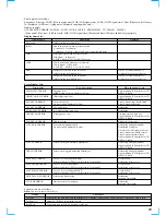
Display Items List:
Display items
Description
Remarks
Error name
t
Refer to the error display list
IN SW
Sled in switch state when an error occurred
0: switch off Not limit in
1: switch on Limit in (Optical pick-up is at most inward track)
FOK
FOK signal state when an error occurred
FOK signal Is focus on?
0: FOK L (Focus off), 1: FOK H (Focus on)
LOCK
LOCK signal state when an error occurred.
LOCK signal Is PLL lock?
0: LOCK L Not lock, 1: LOCK H Lock
From
Displayed if effective in the error item
Disc PSN (relative address) is
t
Refer to the error display list
displayed in case of access error
To
Displayed if effective in the error item
Disc PSN (relative address) is
t
Refer to the error display list
displayed in case of access error
Error Display List:
Error display
Error description
Main causes of errors
DISC DETECT ERROR
Disc type error
Optical pick-up, RF amplifier or CD
MIRR measured time is displayed in From:
DSP IC is faulty
OFFSET ADJUST ERROR
Offset adjustment error
Optical pick-up, RF amplifier or CD
DSP IC is faulty
FCS SRV ON ERROR
Focus servo error
From:1 means focus search failed
An error code is displayed in From:
From:2 means defocusing
CLV SRV ON ERROR
CLV servo error
Defocusing
E-F BALANCE ERROR
E-F balance adjustment error
Defocusing
TRK SRV ON ERROR
Tracking servo error
Tracking servo on time out
Optical pick-up, RF amplifier or CD
DSP IC is faulty
SLD SRV ON ERROR
Sled servo error
Sled servo on time out
FOCUS BIAS ERROR
Focus bias adjustment failed
Defocusing during adjustment
An error code is displayed in From:
Description of display
An error code is displayed in From
From:1 means retry failed 3 times
From:2 means abnormal value
Optical pick-up, RF amplifier or CD
DSP IC is faulty
FCS AGC ERROR
Error at focus gain automatic adjustment
Defocusing during adjustment
Optical pick-up, RF amplifier or CD
DSP IC is faulty
TRK AGC ERROR
Error at tracking gain automatic adjustment
Defocusing during adjustment
Optical pick-up, RF amplifier or CD
DSP IC is faulty
ACCESS 1TJ ERROR
Access Error at one-track jump
Access failed
Effective addresses (PSN) are displayed in From: and To:
Defocusing at access, etc
ACCESS FINE ERROR
Access Error at fine search
Access failed
Effective addresses (PSN) are displayed in From: and To:
Defocusing at access, etc
ACCESS MOVE ERROR
Access Error at M-track MOVE
Access failed
Effective addresses (PSN) are displayed in From: and To:
Defocusing at access, etc
WHILE PLAYING ERROR
Error during disc playing
Defocusing
Focusing retry failed
FCS JUMP ERROR
Time out error at focus jump
Defocusing
Focusing retry failed
System errors are as follows.
Note:
This error is not saved in the set.
Display
Description
Toc Error *
Error during the time from auto adjustment to TOC reading, Different type of disc (Such as a DVD disc), Disc is dirty
Toc Error ****
Illegal SACD (Such as a pirated version)
Read Error
Music data read error (Error during disc playing)
Error display is as follows.
Error name, Disc type, IN SW (Sled in switch state), FOK (FOK signal state), LOCK (LOCK signal state), From (Displayed if effective),
To (Displayed if effective), Aging times (Displayed in aging mode only)
Display example
ACCESS MOVE ERROR : SACDSL : IN SW 1 FOK 0 LOCK 0 : FROM 205663 : TO 2461601 : TIMES 5
(Error name) (Disc type) (Sled in switch, FOK, LOCK signal state) (Relative address) (Relative address)(Aging times)
Содержание SCD-C333ES - Super Audio Cd Changer
Страница 18: ...SCD C333ES 18 18 4 2 SCHEMATIC DIAGRAM RF SECTION Refer to page 40 for Waveforms ...
Страница 22: ...SCD C333ES 22 22 4 6 SCHEMATIC DIAGRAM MAIN SECTION 1 5 Refer to page 49 for IC Pin Function PIN FUNCTION ...
Страница 28: ...SCD C333ES 28 28 4 12 SCHEMATIC DIAGRAM AUDIO SECTION 2 3 ...
Страница 29: ...SCD C333ES 29 29 4 13 SCHEMATIC DIAGRAM AUDIO SECTION 3 3 ...
Страница 31: ...SCD C333ES 31 31 4 15 PRINTED WIRING BOARD AUDIO SECTION SIDE B Refer to page 12 for Circuit Board Location ...
Страница 32: ...SCD C333ES 32 32 4 16 SCHEMATIC DIAGRAM DISPLAY SECTION Refer to page 45 for IC Block Diagrams ...
Страница 34: ...SCD C333ES 34 34 4 18 SCHEMATIC DIAGRAM HP SECTION ...
Страница 36: ...SCD C333ES 36 36 4 20 SCHEMATIC DIAGRAM SENSOR SECTION Refer to page 45 for IC Block Diagram ...
Страница 38: ...SCD C333ES 38 38 4 22 SCHEMATIC DIAGRAM POWER SECTION ...

