


– 40 –
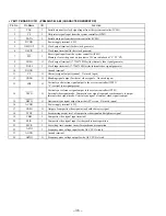
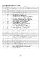
Pin No.
Pin Name
I/O
Function
39 to 44
LED016 to LED021
O
LED drive signal output terminal Not used (open)
45
RMC SEL
I
Not used (fixed at “L”)
46
RMC SEL
—
Not used (open)
47
VCC
—
Power supply terminal (+5V)
48 to 55
SEG15 to SEG08
O
LCD segment drive signal output terminal Not used (open)
56
VSS
—
Ground terminal
57 to 64
SEG07 to SEG00
O
LCD segment drive signal output terminal Not used (open)
65 to 68
V3 to V0
I
Bias voltage input for the LCD drive Not used
69 to 72
COM0 to COM3
O
LCD common drive signal output terminal Not used (open)
73
CG SDE
I
Input of check signal whether vertical sync signal is present or not from character generator
(IC101) “L”: vertical sync signal is present
74
DD CHARGE
O
Charge mode on/off control signal output to the DC/DC converter (IC301)
75
DATA TO MASTER
I
Serial data input from the EEPROM (IC901)
76
DATA TO SLAVE
O
Serial data output to the character generator (IC101), D/A converter (IC202) and EEPROM
(IC901)
77
MODECON SCK
O
Serial data transfer clock signal output to the character generator (IC101), D/A converter
(IC202, 402) and EEPROM (IC901)
78
CS CG
O
Chip select signal output to the character generator (IC101)
79
DD MAIN
O
Main power supply control signal output to the DC/DC converter (IC301)
80
SHUTTER
O
Rectangle waveform (125 Hz) output for the shutter Not used (open)
81
AVSS
—
Ground terminal (for A/D input)
82
MENU/EXEC A/D
I
S702 and S703 keys input on the SA-52P board
83
BATT SIG
I
Not used
84
CHARGE A/D IN
I
Input of battery voltage detection in charge mode (A/D input)
85
BATT SENCE
I
Input of battery capacity detection when rechargeable battery is used (A/D input)
86
DC IN A/D
I
Input of voltage detection when DC adapter is used (A/D input)
87
VOL I/F A/D
—
Not used (open)
88
VOL DS A/D
I
Volume control input terminal (A/D input)
89
P97/AN07
—
Not used (open)
90
AVCC
—
Power supply terminal (+5V) (for A/D input)
91
CS EEPROM
O
Chip select signal output to the EEPROM (IC902)
92
WE EEPROM
O
Data write enable signal output to the EEPROM (IC902)
93
CS DA
O
Chip select signal output to the D/A converter (IC202, 402)
94
PA3/AN11
—
Not used (open)
95
LANC IN
I
LANC serial data input terminal (for test)
96
LANC OUT
O
LANC serial data output terminal (for test)
97
BUZZER
O
Buzzer sound output terminal Not used (open)
98
BACK UP VCC
—
Power supply terminal (+5V)
99
CL1
O
Sub system clock output terminal (32.768 kHz)
100
CL0
I
Sub system clock input terminal (32.768 kHz)
Содержание PLM-A55E
Страница 1: ...SERVICE MANUAL GLASSTRON AEP Model UK Model SPECIFICATIONS PLM A55E 9 928 101 31 ...
Страница 3: ... 3 SECTION 1 GENERAL This section is extracted from instruction manual ...
Страница 4: ... 4 ...
Страница 5: ... 5 ...
Страница 6: ... 6 ...
Страница 7: ... 7 ...
Страница 8: ... 8 ...
Страница 9: ... 9 ...
Страница 10: ... 10 ...
Страница 11: ... 11 ...
Страница 12: ... 12 ...
Страница 13: ... 13 ...
Страница 14: ... 14 ...
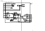
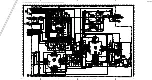
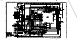
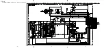
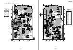
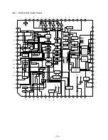
Страница 48: ... 64 65 66 4 11 SCHEMATIC DIAGRAM SA 52P Board See page 75 for IC Block Diagrams PLM A55E Page 57 ...


