background image

9

Introduction

i-3 V2 I/O Controller provides a set of control 
input terminals for wiring devices, such as 
wall switches, photocells or occupancy 
sensors. These terminals are located in the 
input wiring section of the  I/O printed 
circuit board. There are two types of inputs 
provided by these terminals:

 • 

Switch inputs

 – The i-3 V2 I/O Controller  


provides up to 20 input  connections for  


dry or wet (24 VDC) contacts (such as  


wall switches, occupancy sensors, etc).  


These contact inputs are capable of 


acting either independently or in pairs 


to turn ON and OFF. The controller can 


accept  up to 10 three-wire inputs or any 


combination of two- and three-wire 


inputs until its capacity is reached.


• 

Analog I/O 

– i-3 V2 I/O Controller 


provides two analog input and two


analog output connections to control  


0-10V dimming ballast. 

There are two Analog Inputs (at TB6 on the 
I/O Board) and two Analog Outputs (at TB5). 
The Analog Inputs can be used to read any 
0 to 10 Volt input value, and the Analog 
Outputs can be used to drive out 0 to 10 
volts ballast at a maximum of 100 mA each. 
In a practical sense, this means that each 
Analog Output can drive approximately 50 
typical dimming ballasts (assuming each 
ballast uses 2 mA – check your ballast 
documentation for an actual determination). 

The Analog Inputs can be used in any
situation where digital inputs are used. 
They are specified by using input numbers 
33 and 34, but whether they are “ON” or 
“OFF” is more complex. For each analog 
input, registers 20 and 21 give the input 
value in the range 0-4095. Registers 36 
and 37 specify values to be compared 
to the Analog Inputs and comparison 
operations, to determine whether the 
Analog Input is ON or OFF. 

Register 36 is the Compare definition for 
Analog Input 1 (input number 33), and 
contains the comparison value in the 
bottom 12 bits (least significant, bits 
0-11, range 0-4095). The high-order bit 
(bit 15) in that register stands for “equal” 
comparison, bit 14 stands for “less,” and bit 
13 stands for “greater.” These three bits may 
be combined to make “less or equal” or 
“greater or equal” or “always ON” (all three 
bits on). If all three bits are off, then the 
Analog Input is never ON. Register 37
controls the comparison operation for 
Analog Input 2 (input number 34).

Controlling the Analog Outputs: 

Registers


38 and 39 give the actual, read only values 
of the Analog Outputs 1 and 2. Like all 
Analog values, they are a number in the 
range 0 to 4095, corresponding to 0 to 10 
Volts. (NOTE: The actual output may be 
limited by the circuitry to  approximately 
9.2 Volts.)

Registers 22 and 23 are for specifying
Analog Output 1 Set value and Analog
Output 2 Set value. These Set values are
intended to be used to drive the Analog
Outputs. However, whether these Set 
values are used by the Analog Outputs
depends on the Analog Output Feed
registers, 32 and 33.

Each Analog Output’s actual output value 
can be tied to an Analog Input or to register 
22 or 23, but not both. The Analog Output 
Feed registers determine this tie-in. Register 
32 (Analog Output 1 Feed) contains the 
number of the Input to be tied to the 
Analog Output. This number is from 0 to 
44, where 0 is “no connection” and 1-20 
are digital inputs, while numbers of 33 and 
34 are analog inputs 1 and 2. These two 
analog inputs act as a digital inputs based 
on the Analog compare  register values.

Numbers 35 and 36 specify the analog
inputs and the feed is through the direct
values of the analog inputs. Numbers 37
and 38 specify the analog inputs and the
feed is through the difference of the Max
Voltage (4095) and the direct values of
the inputs.

Numbers 39 and 40 do not represent an
actual input, but instead ties this Analog 
Output to register 22 or 23, respectively. 
Register 33 is for specifying the Analog 
Output 2 Feed. Numbers 42 and 42 specify 
the use of the analog gain table. Numbers 
43 and 44 specify the use of the PID loop 
function with values E0 and E1 respectively.

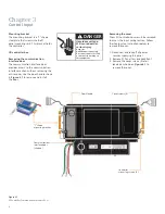
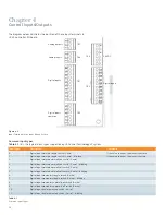
Chapter 4

Control Inputs/Outputs

Figure 4-1

Input / Output Connectors

Input / output connectors

Common

Digital inputs

Analog I/0

24 VDC

Содержание i-3

Страница 1: ...3 User Guide www usa siemens com i 3 i 3 V2 I O Controller Modbus ...

Страница 2: ... involved In addition this person has the following qualifications a is trained and authorized to de energize clear ground and tag circuits and equipment in accordance with established safety practices b is trained in the correct care and use of protective equipment such as rubber gloves hard hat safety glasses or face shields flash clothing etc in accordance with established safety practices c is...

Страница 3: ...te Inputs Input Registers and Holding Registers Address Tables 22 44 D Dimming Instructions 45 47 E USB to RS485 Converter Driver Software Installations Instructions 48 52 F Recommended Input Devices 53 72 G Common Networking setups 73 74 Customer Support Information 75 These instructions do not purport all details or variations in equipment nor to provide for every possible contingency to be met ...

Страница 4: ...a slave panel to accept dry contact or wet digital inputs and analog inputs or commands through communications network by a Building Automation System It provides up to 20 two wire dry or wet contact inputs and two analog inputs which can be used to control up to 42 outputs All SIPOD ON P1 Box Data Rail Ribbon Cable BQD SIPOD Data Rail Ribbon Cable Input Terminals I O Board PC or BAS Modbus Interf...

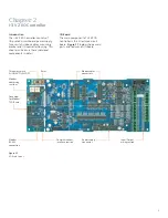
Страница 5: ...al components in detail Figure 2 1 I O Board Layout I O Board The main component of i 3 V2 I O Controller is the I O printed circuit board Figure 2 1 below shows main parts and features of I O Board Ribbon cables connectors Reset Three way switch All ON AUTO ALL OFF Modbus addressing switches Modbus RS 485 connection Connector for Modbus TCP IP card Communications interface section Power supply co...

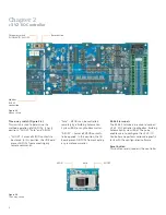
Страница 6: ...nsors 24 VDC TB4 Power supply for sensors light motion etc as well as for wet contacts Firmware upgrade connector This connection is used for Factory Service and is not available to users Ribbon cable connector There are two ribbon cable connectors on the I O Board that interface with the data rails located on each side of the P1 Series Lighting Panel For safety purposes ribbon cables have a key f...

Страница 7: ...5 Chapter 2 i 3 V2 I O Controller Figure 2 4 USB Converter Kit USB RS485 converter kit Part No 5WG1715 8XY02 Phoenix connector Part No 1984028 FTD chip Part No USB RS485 WE 1800 BT ...

Страница 8: ...contacts to be opened In this position the I O Board prevents SIPODs from accepting any remote commands RS 485 terminals The RS 485 terminals are used to connect i 3 V2 I O Controller to a Modbus Building Automation System BAS They also enable users to configure the i 3 V2 I O Controller and perform various diagnostic tests with the configuration software Reset button This button resets reboots th...

Страница 9: ... i 3 V2 controller Be sure to turn the power switch OFF prior to removing the fuse from the controller Ribbon cables A pair of 26 wire ribbon cables connect the I O Board and the data rails They provide two way data communication between the I O Board and SIPODs They also provide power and ground Each ribbon cable has identical connectors on each end A keying feature reduces the risk of installing...

Страница 10: ... Controller cover must be removed to access the input wiring section Follow the step by step instructions below to remove the cover 1 Disconnect and lock off all power sources supplying this panel 2 Remove P1 Panel trim and deadfront 3 Remove the cover screws 4 total located as shown on Figure 3 1 to remove the cover DANGER Hazardous voltage Will cause death or serious injury Keep out Qualified per...

Страница 11: ...al comparison bit 14 stands for less and bit 13 stands for greater These three bits may be combined to make less or equal or greater or equal or always ON all three bits on If all three bits are off then the Analog Input is never ON Register 37 controls the comparison operation for Analog Input 2 input number 34 Controlling the Analog Outputs Registers 38 and 39 give the actual read only values of...

Страница 12: ...inking if the value changes then invert the state 2 Digital input maintain normally on switch 2 wire 3 Digital input maintain normally on switch 2 wire blinking 4 Digital input maintain normally off switch 2 wire 5 Digital input maintain normally off switch 2 wire blinking 6 Digital input momentary toggle switch 2 wire 7 Digital input momentary toggle switch 2 wire blinking 8 Digital input momenta...

Страница 13: ... output mapping Setting input output mapping can be accomplished using Modbus communication protocol or the configuration software Any given input to the I O Board may be connected to one output or to an output group or zone which is more than one output Refer to Modbus Map table in Chapter 5 Communication Protocols under Configuring i 3 V2 I O Controller section for more information ...

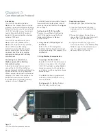
Страница 14: ...shown in Figure 5 1 The RS 485 terminal is accessible through Communication Interface Door without removing the panel deadfront See Figure 3 1 on page 8 Configuring i 3 V2 I O Controller There are two methods of configuring i 3 V2 I O Controller using The Panel Configurator Software or Modbus communications 1 Using the i 3 V2 I O Configurator Software Refer to i 3 V2 I O Configurator Software Tool...

Страница 15: ... Controller input to output mapping is not set Input to Output mapping can be redefined as desired to meet the project specification To map input to output follow these steps 1 Use either function code 6 preset single register or 16 preset multiple registers 2 Register address for input to output map starts from 2048 for input terminal 1 to 2067 for input terminal 32 3 Assign the register value fo...

Страница 16: ...eared All three of these flags mean that there was a problem since the last time a status was sent to the I O Board not necessarily related to the previous message from the I O Board For example if the I O Board requests an Open then a Close then sends GetStatus and the status contains a FAIL flag then either the Open or the Close failed or both but the I O Board cannot determine which operation f...

Страница 17: ...igital inputs or 33 analog input 1 or 34 for analog input 3 in the second byte A value of 0 in a register means that there is no Logic operation to be applied A Logic operation allows the user to relate two different inputs to a POD with an AND OR NAND or XOR logical connection NOTE A special situation can occur when two inputs are linked to each other and one has an OR operation and the other has...

Страница 18: ...e saved to flash memory so they can be recovered after the system is reset and or after the power is turned OFF and back ON These are the registers that are saved to Flash memory Register Description 32 39 Analog configuration 106 Number of flash writes 107 110 Analog Output Correction factors 116 Analog Input 1 Hysteresis 117 Analog Input 1 Epsilon 120 Modbus device address 121 123 RS 485 baud ra...

Страница 19: ...able Appendix C Modbus Coils Discrete Inputs Input Registers and Holding Registers Address Tables Appendix D Dimming Instructions Appendix E USB to RS485 Converter Driver Software Installations Instructions Appendix F Recommended input devices Appendix G Common Networking setups ...

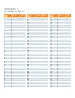
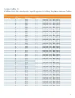
Страница 20: ... 60 3 c 61 3 d 62 3 e 63 3 f 64 4 0 65 4 1 66 4 2 67 4 3 68 4 4 69 4 5 70 4 6 71 4 7 72 4 8 73 4 9 74 4 a 75 4 b 76 4 c 77 4 d 78 4 e 79 4 f 80 5 0 81 5 1 82 5 2 83 5 3 84 5 4 85 5 5 86 5 6 87 5 7 88 5 8 89 5 9 90 5 a 91 5 b 92 5 c 93 5 d 94 5 e 95 5 f 96 6 0 97 6 1 98 6 2 99 6 3 100 6 4 Modbus Address Dip Switch 1 S4 Dip Switch 2 S5 101 6 5 102 6 6 103 6 7 104 6 8 105 6 9 106 6 a 107 6 b 108 6 c ...

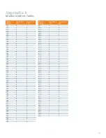
Страница 21: ... 8 185 b 9 186 b a 187 b b 188 b c 189 b d 190 b e 191 b f 192 c 0 193 c 1 194 c 2 195 c 3 196 c 4 197 c 5 198 c 6 199 c 7 200 c 8 Modbus Address Dip Switch 1 S4 Dip Switch 2 S5 201 c 9 202 c a 203 c b 204 c c 205 c d 206 c e 207 c f 208 d 0 209 d 1 210 d 2 211 d 3 212 d 4 213 d 5 214 d 6 215 d 7 216 d 8 217 d 9 218 d a 219 d b 220 d c 221 d d 222 d e 223 d f 224 e 0 225 e 1 226 e 2 227 e 3 228 e ...

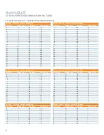
Страница 22: ...rtical numbering Circuit No Modbus Addr Circuit No Modbus Addr 1 0 16 21 2 1 17 22 3 2 18 23 4 3 19 24 5 4 20 25 6 5 21 26 7 6 22 27 8 7 23 28 9 8 24 29 Bottom feed 42 circuits vertical numbering Circuit No Modbus Addr Circuit No Modbus Addr 1 41 22 20 2 40 23 19 3 39 24 18 4 38 25 17 5 37 26 16 6 36 27 15 7 35 28 14 8 34 29 13 9 33 30 12 10 32 31 11 11 31 32 10 12 30 33 9 13 29 34 8 14 28 35 7 15...

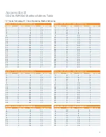
Страница 23: ...zontal numbering Circuit No Modbus Addr Circuit No Modbus Addr 1 0 2 21 3 1 4 22 5 2 6 23 7 3 8 24 9 4 10 25 11 5 12 26 13 6 14 27 15 7 16 28 17 8 18 29 Bottom feed 42 circuits horizontal numbering Circuit No Modbus Addr Circuit No Modbus Addr 1 41 2 20 3 40 4 19 5 39 6 18 7 38 8 17 9 37 10 16 11 36 12 15 13 35 14 14 15 34 16 13 17 33 18 12 19 32 20 11 21 31 22 10 23 30 24 9 25 29 26 8 27 28 28 7 ...

Страница 24: ...0 Close 1 27 00028 0 1 SIPOD 28 Open 0 Close 1 28 00029 0 1 SIPOD 29 Open 0 Close 1 29 00030 0 1 SIPOD 30 Open 0 Close 1 30 00031 0 1 SIPOD 31 Open 0 Close 1 31 00032 0 1 SIPOD 32 Open 0 Close 1 32 00033 0 1 SIPOD 33 Open 0 Close 1 33 00034 0 1 SIPOD 34 Open 0 Close 1 34 00035 0 1 SIPOD 35 Open 0 Close 1 35 00036 0 1 SIPOD 36 Open 0 Close 1 36 00037 0 1 SIPOD 37 Open 0 Close 1 37 00038 0 1 SIPOD 3...

Страница 25: ...tput Group Zone 35 Open 0 Close 1 99 00100 0 1 Output Group Zone 36 Open 0 Close 1 100 00101 0 1 Output Group Zone 37 Open 0 Close 1 101 00102 0 1 Output Group Zone 38 Open 0 Close 1 102 00103 0 1 Output Group Zone 39 Open 0 Close 1 103 00104 0 1 Output Group Zone 40 Open 0 Close 1 104 00105 0 1 Output Group Zone 41 Open 0 Close 1 105 00106 0 1 Output Group Zone 42 Open 0 Close 1 106 00107 0 1 Out...

Страница 26: ...igital Input 17 Off 0 On 1 17 10018 0 1 Digital Input 18 Off 0 On 1 18 10019 0 1 Digital Input 19 Off 0 On 1 19 10020 0 1 Digital Input 20 Off 0 On 1 20 10021 0 1 Digital Input 21 Off 0 On 1 21 10022 0 1 Digital Input 22 Off 0 On 1 22 10023 0 1 Digital Input 23 Off 0 On 1 23 10024 0 1 Digital Input 24 Off 0 On 1 24 10025 0 1 Digital Input 25 Off 0 On 1 25 10026 0 1 Digital Input 26 Off 0 On 1 26 1...

Страница 27: ... 0 On 1 Bit 15 Digital Input 16 Off 0 On 1 1 30002 Bit 0 Digital Input 17 Off 0 On 1 Bit 1 Digital Input 18 Off 0 On 1 Bit 2 Digital Input 19 Off 0 On 1 Bit 3 Digital Input 20 Off 0 On 1 Bit 4 Digital Input 21 Off 0 On 1 Bit 5 Digital Input 22 Off 0 On 1 Bit 6 Digital Input 23 Off 0 On 1 Bit 7 Digital Input 24 Off 0 On 1 Bit 8 Digital Input 25 Off 0 On 1 Bit 9 Digital Input 26 Off 0 On 1 Bit 10 Di...

Страница 28: ...ask for SIPOD 20 Open 0 Close 1 Bit 4 Mask for SIPOD 21 Open 0 Close 1 Bit 5 Mask for SIPOD 22 Open 0 Close 1 Bit 6 Mask for SIPOD 23 Open 0 Close 1 Bit 7 Mask for SIPOD 24 Open 0 Close 1 Bit 8 Mask for SIPOD 25 Open 0 Close 1 Bit 9 Mask for SIPOD 26 Open 0 Close 1 Bit 10 Mask for SIPOD 27 Open 0 Close 1 Bit 11 Mask for SIPOD 28 Open 0 Close 1 Bit 12 Mask for SIPOD 29 Open 0 Close 1 Bit 13 Mask fo...

Страница 29: ...SIPOD 25 Open 0 Close 1 Bit 9 SIPOD 26 Open 0 Close 1 Bit 10 SIPOD 27 Open 0 Close 1 Bit 11 SIPOD 28 Open 0 Close 1 Bit 12 SIPOD 29 Open 0 Close 1 Bit 13 SIPOD 30 Open 0 Close 1 Bit 14 SIPOD 31 Open 0 Close 1 Bit 15 SIPOD 32 Open 0 Close 1 6 4007 Bit 0 SIPOD 33 Open 0 Close 1 Bit 1 SIPOD 34 Open 0 Close 1 Bit 2 SIPOD 35 Open 0 Close 1 Bit 3 SIPOD 36 Open 0 Close 1 Bit 4 SIPOD 37 Open 0 Close 1 Bit...

Страница 30: ...POD 31 Exists 1 Not Exists 0 Bit 15 SIPOD 32 Exists 1 Not Exists 0 10 40011 Bit 0 SIPOD 33 Exists 1 Not Exists 0 Bit 1 SIPOD 34 Exists 1 Not Exists 0 Bit 2 SIPOD 35 Exists 1 Not Exists 0 Bit 3 SIPOD 36 Exists 1 Not Exists 0 Bit 4 SIPOD 37 Exists 1 Not Exists 0 Bit 5 SIPOD 38 Exists 1 Not Exists 0 Bit 6 SIPOD 39 Exists 1 Not Exists 0 Bit 7 SIPOD 40 Exists 1 Not Exists 0 Bit 8 SIPOD 41 Exists 1 Not ...

Страница 31: ...POD 35 Failure 1 Non Failure 0 Mode Bit 3 SIPOD 36 Failure 1 Non Failure 0 Mode Bit 4 SIPOD 37 Failure 1 Non Failure 0 Mode Bit 5 SIPOD 38 Failure 1 Non Failure 0 Mode Bit 6 SIPOD 39 Failure 1 Non Failure 0 Mode Bit 7 SIPOD 40 Failure 1 Non Failure 0 Mode Bit 8 SIPOD 41 Failure 1 Non Failure 0 Mode Bit 9 SIPOD 42 Failure 1 Non Failure 0 Mode Bit 10 Not Used Bit 11 Not Used Bit 12 Not Used Bit 13 N...

Страница 32: ...l for Digital Input 11 Off 0 On 1 Bit 11 Control for Digital Input 12 Off 0 On 1 Bit 12 Control for Digital Input 13 Off 0 On 1 Bit 13 Control for Digital Input 14 Off 0 On 1 Bit 14 Control for Digital Input 15 Off 0 On 1 Bit 15 Control for Digital Input 16 Off 0 On 1 19 40020 Bit 0 Control for Digital Input 17 Off 0 On 1 Bit 1 Control for Digital Input 18 Off 0 On 1 Bit 2 Control for Digital Inpu...

Страница 33: ...pen 0 Close 1 Bit 10 Mask for Output Group Zone 27 Open 0 Close 1 Bit 11 Mask for Output Group Zone 28 Open 0 Close 1 Bit 12 Mask for Output Group Zone 29 Open 0 Close 1 Bit 13 Mask for Output Group Zone 30 Open 0 Close 1 Bit 14 Mask for Output Group Zone 31 Open 0 Close 1 Bit 15 Mask for Output Group Zone 32 Open 0 Close 1 26 40027 Bit 0 Mask for Output Group Zone 33 Open 0 Close 1 Bit 1 Mask for...

Страница 34: ...1 Bit 15 Output Group Zone 16 Open 0 Close 1 29 40030 Bit 0 Output Group Zone 17 Open 0 Close 1 Bit 1 Output Group Zone 18 Open 0 Close 1 Bit 2 Output Group Zone 19 Open 0 Close 1 Bit 3 Output Group Zone 20 Open 0 Close 1 Bit 4 Output Group Zone 21 Open 0 Close 1 Bit 5 Output Group Zone 22 Open 0 Close 1 Bit 6 Output Group Zone 23 Open 0 Close 1 Bit 7 Output Group Zone 24 Open 0 Close 1 Bit 8 Outp...

Страница 35: ...are see Analog In Out 38 40039 Analog Output 1 Actual read only see Analog In Out 39 40040 Analog Output 2 Actual read only see Analog In Out 40 40041 SIPOD 1 Status word See SIPOD Status Read Only 41 40042 SIPOD 2 Status word See SIPOD Status Read Only 42 40043 SIPOD 3 Status word See SIPOD Status Read Only 43 40044 SIPOD 4 Status word See SIPOD Status Read Only 44 40045 SIPOD 5 Status word See S...

Страница 36: ...Reserved 104 40105 I O Board Milliseconds Timer 0 60000 Read Only 105 40106 I O Board Minutes Timer 0 65000 Read Only 106 40107 Number of flash writes of parameters since the last complete program reload from JTAG 107 40108 Analog Output 1 Linear Correction 0 2048 default 0 108 40109 Analog Output 1 Voltage Percentage Correction 0 100 default 0 109 40110 Analog Output 2 Linear Correction 0 2048 def...

Страница 37: ...e definition 24 280 40281 Output Group Zone definition 25 281 40282 Output Group Zone definition 26 282 40283 Output Group Zone definition 27 283 40284 Output Group Zone definition 28 284 40285 Output Group Zone definition 29 285 40286 Output Group Zone definition 30 286 40287 Output Group Zone definition 31 287 40288 Output Group Zone definition 32 288 40289 Output Group Zone definition 33 289 40290 Output...

Страница 38: ... definition 77 333 40334 Output Group Zone definition 78 334 40335 Output Group Zone definition 79 335 40336 Output Group Zone definition 80 336 40337 Output Group Zone definition 81 337 40338 Output Group Zone definition 82 338 40339 Output Group Zone definition 83 339 40340 Output Group Zone definition 84 340 40341 Output Group Zone definition 85 341 40342 Output Group Zone definition 86 342 40343 Output ...

Страница 39: ...It is advisable to select more than 60 seconds as Blink time 778 40779 BlinkCycle 0 15000 s time in seconds for the blinking off on cycle i e frequency of blinking default 60 Note It is advisable to select 30 or more seconds as blink cycle 779 40780 BlinkOffTime 0 255 s time in seconds that the lights are turned off in each cycle default 1 780 40781 Reserved 781 40782 Time in minutes to check for ...

Страница 40: ... 14 Status 2nd pole if Two Three Pole 0 Open 1 Closed Bit 13 Status 3rd pole if Three Pole 0 Open 1 Closed Bit 10 12 Not used Bit 8 9 SIPOD Type 1 Single Pole 2 Two Pole 3 Three Pole Bit 0 7 SIPOD position number data rail port number 1516 41517 Bit 15 Status 0 Open 1 Closed SIPOD 42 Report Bit 8 14 Other flags Bit 0 7 Version 0 Open 1 Closed 1517 41518 Timestamp Minutes 1518 41519 Timestamp Ticks ...

Страница 41: ...ital Input 21 Type 1813 41814 Digital Input 22 Type 1814 41815 Digital Input 23 Type 1815 41816 Digital Input 24 Type 1816 41817 Digital Input 25 Type 1817 41818 Digital Input 26 Type 1818 41819 Digital Input 27 Type 1819 41820 Digital Input 28 Type 1820 41821 Digital Input 29 Type 1821 41822 Digital Input 30 Type 1822 41823 Digital Input 31 Type 1823 41824 Digital Input 32 Type 1824 41825 Reserve...

Страница 42: ...0 42081 O Map for Analog Input 1 2081 42082 I O Map for Analog Input 2 2082 2303 Reserved 2304 42305 Byte 1 I O Controller Status Byte 2 I O Controller Firmware Version 2305 42306 Minutes since IO Controller started rolls over to 0 at 65000 2306 42307 Milliseconds since IO Controller started rolls over to 0 at 60000 2307 42308 Reserved 2308 42309 Reserved 2309 42310 Reserved 2310 42311 Number of g...

Страница 43: ...it 8 15 Type of SIPOD 5 Bit 0 7 Type of SIPOD 6 2819 42820 Bit 8 15 Type of SIPOD 7 Bit 0 7 Type of SIPOD 8 2820 42821 Bit 8 15 Type of SIPOD 9 Bit 0 7 Type of SIPOD 10 2821 42822 Bit 8 15 Type of SIPOD 11 Bit 0 7 Type of SIPOD 12 2822 42823 Bit 8 15 Type of SIPOD 13 Bit 0 7 Type of SIPOD 14 2823 42824 Bit 8 15 Type of SIPOD 15 Bit 0 7 Type of SIPOD 16 2824 42825 Bit 8 15 Type of SIPOD 17 Bit 0 7 ...

Страница 44: ... for Input 16 3088 43089 Timed override for Input 17 3089 43090 Timed override for Input 18 3090 43091 Timed override for Input 19 3091 43092 Timed override for Input 20 3092 43093 Timed override for Input 21 3093 43094 Timed override for Input 22 3094 43095 Timed override for Input 23 3095 43096 Timed override for Input 24 3096 43097 Timed override for Input 25 3097 43098 Timed override for Input...

Страница 45: ... Override time SIPOD 32 3360 43361 Override time SIPOD 33 3361 43362 Override time SIPOD 34 3362 43363 Override time SIPOD 35 3363 43364 Override time SIPOD 36 3364 43365 Override time SIPOD 37 3365 43366 Override time SIPOD 38 3366 43367 Override time SIPOD 39 3367 43368 Override time SIPOD 40 3368 43369 Override time SIPOD 41 3369 43370 Override time SIPOD 42 3370 3583 Reserved 3584 43585 Logic ...

Страница 46: ...607 Logic Operation for Digital Input 23 3607 43608 Logic Operation for Digital Input 24 3608 43609 Logic Operation for Digital Input 25 3609 43610 Logic Operation for Digital Input 26 3610 43611 Logic Operation for Digital Input 27 3611 43612 Logic Operation for Digital Input 28 3612 43613 Logic Operation for Digital Input 29 3613 43614 Logic Operation for Digital Input 30 3614 43615 Logic Operat...

Страница 47: ...el Setting 3 0 4095 8205 Analog Input Threshold Level Setting 4 0 4095 8206 Analog Input Threshold Level Setting 5 0 4095 8207 Analog Input Threshold Level Setting 6 0 4095 8208 Analog Input Threshold Level Setting 7 0 4095 8209 Analog Input Threshold Level Setting 8 0 4095 8210 Analog Input Threshold Level Setting 9 0 4095 8211 Analog Input Threshold Level Setting 10 0 4095 Analog Output Desired ...

Страница 48: ...og Input Threshold Level Setting 3 1229 3v 8205 Analog Input Threshold Level Setting 4 1638 4v 8206 Analog Input Threshold Level Setting 5 2048 5v 8207 Analog Input Threshold Level Setting 6 2457 6v 8208 Analog Input Threshold Level Setting 7 2867 7v 8209 Analog Input Threshold Level Setting 8 3276 8v 8210 Analog Input Threshold Level Setting 9 3686 9v 8211 Analog Input Threshold Level Setting 10 ...

Страница 49: ... Input 2 44 Typical Example Scenario Connect an Analog Light Sensor to the TB6 terminal Analog Input 1 or Analog Input 2 Typically in this scenario the sensor will be pointing to the inside light level Connect a Dimming Ballast to the TB5 terminal Analog Output 1 Set the Analog Output Feed Settings as follows Register 32 value as 43 if the dimming ballasts are connected to Analog Output 1 Register...

Страница 50: ...ftdichip com Drivers CDM CDM20814_Setup exe The following window opens 2 Click on Save to download the exe file CDM20814_Setup exe Save it in any folder of your choice 3 Make sure the USB RS485 cable is unplugged 4 Double click on CDM20814_Setup exe file When the console window goes away the driver is ready The following window appears ...

Страница 51: ...r is ready 7 Plug in the USB RS485 cable and the driver will load 8 To determine which COM port was allotted by the system for this USB to RS485 Converter follow these steps a Be sure the USB to RS485 converter is connected to your system b On the desktop right click on the My Computer Icon c Click on Properties the following window opens ...

Страница 52: ...50 Appendix E USB to RS485 Converter Driver Software Installation Instructions d Click on the Hardware tab the following screen opens e Click on Device manager the following screen opens ...

Страница 53: ...51 Appendix E USB to RS485 Converter Driver Software Installation Instructions f Press the symbol to expand Ports COM LPT to see which virtual COM port is assigned to the USB RS485 converter ...

Страница 54: ...52 Appendix E USB to RS485 Converter Driver Software Installation Instructions ...

Страница 55: ...ary NO 2 Wire 1 Leviton LVS 2W Low voltage switch Momentary Momentary NO 2 Wire 2 Leviton LVS 3W Low voltage switch Momentary Momentary NO 2 Wire 3 Leviton LVS 4W Low voltage switch Momentary Momentary NO 2 Wire 4 Leviton LVS 5W Low voltage switch Momentary Momentary NO 2 Wire 5 Leviton LVS 6W Low voltage switch Momentary Momentary NO 2 Wire 6 Leviton LVS 8W Low voltage switch Momentary Momentary ...

Страница 56: ...pper LS 102 Maintained Requires 24 VDC It is a powered input it inputs 24 DC into the i 3 input or it can be used with an interposing relay Indoor 1 Powered 24 VDC Sensor Switch CM PC Maintained Requires 24 VDC It is a powered input it inputs 24 DC into the i 3 input or it can be used with an interposing relay Indoor 1 Powered 24 VDC Sensor Switch CMR PC CMRB PC Maintained Line voltage it requires...

Страница 57: ...55 Appendix F Recommended Input Devices ...

Страница 58: ...56 Appendix F Recommended Input Devices ...

Страница 59: ...57 Appendix F Recommended Input Devices ...

Страница 60: ...58 Appendix F Recommended Input Devices ...

Страница 61: ...59 Appendix F Recommended Input Devices ...

Страница 62: ...60 Appendix F Recommended Input Devices ...

Страница 63: ...61 Appendix F Recommended Input Devices ...

Страница 64: ...62 Appendix F Recommended Input Devices ...

Страница 65: ...63 Appendix F Recommended Input Devices ...

Страница 66: ...64 Appendix F Recommended Input Devices ...

Страница 67: ...65 Appendix F Recommended Input Devices ...

Страница 68: ...66 Appendix F Recommended Input Devices ...

Страница 69: ...67 Appendix F Recommended Input Devices ...

Страница 70: ...68 Appendix F Recommended Input Devices ...

Страница 71: ...69 Appendix F Recommended Input Devices ...

Страница 72: ...70 Appendix F Recommended Input Devices ...

Страница 73: ...71 Appendix F Recommended Input Devices ...

Страница 74: ...72 Appendix F Recommended Input Devices ...

Страница 75: ...73 Appendix G Common Networking Setups ...

Страница 76: ...74 Appendix G Common Networking Setups ...

Страница 77: ...rt Call us at 1 800 333 7421 or visit www usa siemens com powerdistribution i 3 Web site www usa siemens com i 3 For Nearest Sales Office Call us at 1 800 964 4114 or visit www usa siemens com i 3 Warranty Support and Customer Service http www3 sea siemens com sales salesoffices html rc 1 Contact local sales office ...

Страница 78: ...76 Notes ...

Страница 79: ......

Страница 80: ...ions or characteristics of performance which in case of actual use do not always apply as described or which may change as a result of further development of the products An obligation to provide the respective characteristics shall only exist if expressly agreed in the terms of contract All product designations may be trademarks or product names of Siemens AG or supplier companies whose use by th...

Отзывы: