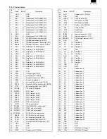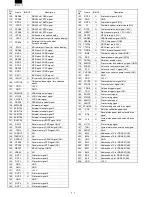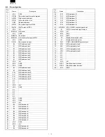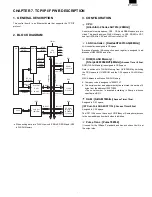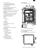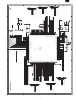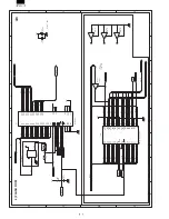
4. MAIN LSI DESCRIPTION
1) CPU (SH7014)
1)-1. SH7014 Overview
The SH7014 CMOS single-chip microprocessors integrate a Hitachi-
original architecture, high-speed CPU with peripheral functions re-
quired for system configuration.
The CPU has a RISC-type instruction set. Most instructions can be
executed in one clock cycle, which greatly improves instruction exe-
cution speed. In addition, the 32-bit internal-bus architecture en-
hances data processing power. With this CPU, it has become possi-
ble to assemble low cost, high performance/high-functioning systems,
even for applications that were previously impossible with microproc-
essors, such as real-time control, which demands high speeds. In
particular, the SH7040 series has a 1-kbyte on-chip cache, which
allows an improvement in CPU performance during external memory
access.
In addition, this LSI includes on-chip peripheral functions necessary
for system configuration, such as large-capacity ROM (except the
SH7014, which is ROMless) and RAM, timers, a serial communica-
tion interface (SCI), an A/D converter, an interrupt controller, and I/O
ports. Memory or peripheral LSIs can be connected efficiently with an
external memory access support function.
This greatly reduces system cost.
1)-1-1. SH7014 Features
CPU:
•
Original Hitachi architecture
•
32-bit internal data bus
•
General-register machine
–
Sixteen 32-bit general registers
–
Three 32-bit control registers
–
Four 32-bit system registers
•
RISC-type instruction set
–
Instruction length: 16-bit fixed length for improved code effi-
ciency
–
Load-store architecture (basic operations are executed be-
tween registers)
–
Delayed branch instructions reduce pipeline disruption during
branch
–
Instruction set based on C language
•
Instruction execution time: one instruction/cycle (35 ns/instruction
at 28.7-MHz operation)
•
Address space: Architecture supports 4 Gbytes
•
On-chip multiplier: multiplication operations (32 bits x 32 bits
64
bits) and multiplication/accumulation operations (32 bits x 32 bits +
64 bits
64 bits) executed in two to four cycles
•
Five-stage pipeline
Cache Memory:
•
1-kbyte instruction cache
•
Caching of instruction codes and PC relative read data
•
4-byte line length (1 longword: 2 instruction lengths)
•
256 entry cache tags
•
Direct map method
•
On-chip RAM, and on-chip I/O areas not objects of cache
•
Used in common with on-chip RAM; 2 kbytes of on-chip RAM used
as address array/data array when cache is enabled
Interrupt Controller (INTC):
•
Seven external interrupt pins (NMI, IRQ x 6)
•
Twenty-eight internal interrupt sources
•
Sixteen programmable priority levels
Bus State Controller (BSC):
•
Supports external extended memory access
–
8-bit, or 16-bit external data bus
•
Memory address space divided into five areas (four areas of
SRAM space, one area of DRAM space) with the following settable
features:
–
Number of wait cycles
–
Outputs chip-select signals for each area
–
During DRAM space access:
•
Outputs RAS and CAS signals for DRAM
•
Can generate a RAS precharge time assurance Tp cycle
•
DRAM burst access function
–
Supports high-speed access mode for DRAM
•
DRAM refresh function
–
Programmable refresh interval
–
Supports CAS-before-RAS refresh and self-refresh modes
•
Wait cycles can be inserted using an external WAIT signal
•
Address data multiplex I/O devices can be accessed
Note: No bus release
Direct Memory Access Controller (DMAC) (2 Channels):
•
Supports cycle-steal and burst transfers
•
Supports single address mode and dual address mode transfers
•
Priority order: fixed at channel 0 > channel 1
•
Transfer counter: 16 bits
•
Transfer request sources: external DREQ input, auto-request, and
on-chip supporting modules
•
Address space: 4 Gbytes
•
Choice of 8-, 16-, or 32-bit transfer data size
Multifunction Timer/Pulse Unit (MTU) (3 Channels):
•
Maximum 8 types of waveform output or maximum 16 types of
pulse I/O processing possible based on 16-bit timer, 3 channels
•
8 dual-use output compare/input capture registers
•
8 independent comparators
•
8 types of counter input clock
•
Input capture function
•
Pulse output mode
–
One shot, toggle, PWM
>>>>> USE FONT <<<<<
Helvetica/ Helvetica-Condensed/ Century-Schoolbook/ Symbol & OriginalFonts: (RingWorld2/RingFont2/Pa
Symbol/PartsCod)
- - - - - - - - - - - - - - - - - - - - - - - - - - - - - - - - - - - - - - - - - - - - - - - - - - - - - - -
Содержание UP-600
Страница 8: ......
Страница 77: ...CHAPTER 9 PWB LAYOUT 1 MAIN PWB 1 A side R VRD RC2EY103J is added IC1 94pin R71 ...
Страница 78: ...2 B side Symbol PartsCod ...
Страница 79: ...2 CKDC PWB 3 DISPLY MCR PWB 1 A side 2 B side 4 RS232 RELAY PWB 1 A side 2 B side ...
Страница 80: ...5 IPL ROM PWB 1 A side 8 POP UP DISPLY 9 LCD I F PWB 2 B side 6 TCP IP RELAY PWB 7 VR PWB ...
Страница 81: ...10 TCP IP I F PWB B side A side ...


