background image

5)-6. PES & NES SENSOR Check

Checking

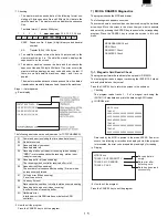
The screen displays the operating status of the paper end sensor
and paper near end sensor of the receipt/journal printer.

Display

Display

Status

Description

NES

0

Senses the near end of the journal paper roll.

1

Does not sense the near end of the journal
paper roll. 

RPES

0

Senses the end of the receipt paper roll.

1

Does not sense the end of the receipt paper roll.

JPES

0

Senses the end of the journal paper roll.

1

Does not sense the end of the journal paper roll.

OPBS

0

IPL ROM PWB connected

1

IPL ROM PWB not connected

How to exit the program

Press the CANCEL key to exit the program.

5)-7. DOT PULSE Adjustment

Checking

The dot width adjustment circuit controls the pulse width of the
current which is added to the printer dot head in response to
fluctuations n supply voltage. If the circuit is replaced with a new
one for any reason such as repair, the dot pulse width needs to be
adjusted using the 200K’s knob VR1. When the DOT PULSE
Adjustment is executed, the dot pulse "PE" is outputted without
printing.

Display

How  to exit the program

Press the CANCEL key to exit the program.

6) TCP/IP STACK NETWORK DIAGNOSTICS 

The program performs the TCP/IP stack test.
The test requirements are as follows:

UP-600

10BASE-T cable (for data transfer testing)

HUB (for loop back test and data transfer test where 2 or more
units are used.) 

The following menu appears. The cursor shown in reverse video can
be moved using the up/down arrow keys. Move the cursor to the
menu item you want to execute and press the ENTER key to execute
the corresponding check program. After the selected Diag. program is
completed, the screen returns to this menu.

Press the CANCEL key to return the screen to the Diag. submenu.

6)-1. SELF Check

Checking

The program executes Diag’s built in TCP/IP stack board and
displays the results.

i. Execute the flash memory test command and display the re-

sult.

ii. Execute the SRAM test command and display the result.

iii. Execute the dual-port RAM test and display the result.

iv. Execute the interrupt test command and display the result.

The information inside the error status is as follows:

b7

Reserved  ("0" is always displayed)

b6

Reserved  ( "0" is always displayed)

b5

Reserved  ("0" is always displayed)

b4

Reserved  ( "0" is always displayed)

b3

HR_RST : If /INTHR cannot be canceled

b2

HR_ACK:If /INTHR does not enter after waiting for 10 ms

b1

HW_RST : If /INTHW cannot be canceled

b0

Reserved  ("0" is always displayed)

Display

How to exit the program.

Press the CANCEL key to exit the program.

NES : 0    (or 1)

RPES : 0   (or 1)

JPES : 0   (or 1)

OPBS : 0   (or 1)

PES&NES SENSOR Check

DOT PULSE Adjustment

DATA Trans.(SA)

DATA Trans.(MA) 

MAC ADDR&FIRM WRITE

MAC ADDR&FIRM Ver. Read 

LOOPBACK Check

SELF Check

TCP/IP DIAG

XXXXXXXX 

INTERRUPT : PASS (or ERROR)

XXXXXXXX : XX :  XX

DPRAM : PASS (or ERROR)

XXXXXXXX : XX :  XX

SRAM : PASS (or ERROR)

FLASH : PASS (or ERROR)

SELF Check

When an error occurs,
the address and data
are displayed.

When an error occurs,
the data is displayed.

When an error occurs,
the address and data
are displayed.

Содержание UP-600

Страница 1: ...DESCRIPTION 6 1 CHAPTER 7 TCP IP I F PWB DESCRIPTION 7 1 CHAPTER 8 CIRCUIT DIAGRAM 8 1 CHAPTER 9 PWB LAYOUT 9 1 CONTENTS Parts marked with are important for maintaining the safety of the set Be sure to replace these parts with specified ones for maintaining the safety and performance of the set SHARP CORPORATION This document has been published to be used for after sales service only The contents ...

Страница 2: ...aneous function key CONV Currency conversion menu key CHK Check Menu Key CH Charge Menu Key SBTL Subtotal Key CA AT Cash amount tendered key Dept 1 to 22 Department 1 to 22 Keys CASH Cashier number entry FS SHIFT Food stamp shift key FS TEND Food stamp tender key NS No sale key TAX Manual tax key NEXT Next higher dollar key MDSE SBTL Merchandise subtotal key AMT Amount entry key TM Non add code Da...

Страница 3: ...artment number key BACK SPACE Back space key TRANS OUT Transfer out key TRANS IN Transfer in key RCP SW Receipt ON OFF key WASTE Waste mode key BS Bill separation key BT Bill totalize bill transfer key CHECK ADD PRINT Validation print key BILL Bill print key PAST VOID Past void key SBTL VOID Subtotal void key GDSC 1 to 3 Group discount 1 to 3 keys COVER CNT Cover count key N C New check key KEY TO...

Страница 4: ... to go back to the previous page CL Used to clear the last setting you have programmed or clear the error state Used to toggle between two or more options SBTL Used to list those options which you can toggle by the key RECALL Used to call up a desired code Numeric keys Used for entering figures 3 DISPLAY 1 OPERATOR DISPLAY Screen example 1 REG mode Price level shift indicator P1 P6 Shows the PLU U...

Страница 5: ...s cashiers clerks to take X or Z reports for their sales information This setting may be used only when your register has been programmed for OP X Z mode available in the PGM2 mode REG For entering sales PGM1 To program those items that need to be changed often e g unit prices of departments PLUs or UPCs and per centages PGM2 To program all PGM1 items and those items that do not require frequent c...

Страница 6: ...er thickness 0 06 to 0 09mm paper weight 52 3 to 64g m2 Validation form Thickness 0 07 to 0 14mm Size 130mm or more W 70mm or more H 4 INKING Ink supply system Ink ribbon Form Cartridge Endless ribbon Specification Material Nylon Ribbon life Approx 6 million characters Print color Purple 5 LOGO STAMP None 6 CUTTER Method Manual 6 DRAWER 1 SPECIFICATION 1 Drawer box and drawer Model name SK 460 Siz...

Страница 7: ...SUB 9pin D SUB 9pin CI 5V selectable ER A6HS1 5V necessary Scanner 5V not necessary Modem PC Printer Scale POS utility 02fd exe The ER A6HS1 cannot be connected to port 2 3 and 4 because it requires 5V The modem cannot be connected to port 2 because it uses a different signal line For the modular RJ45 to D Sub 9pin conversion cable see the following 1 2 3 4 5 6 7 8 9 CD RD SD ER GND DR RS CS CI VC...

Страница 8: ......

Страница 9: ...T NAME MODEL NAME REMARK 1 External printers TM T88 85 TM T88 2 TM T80 TM U200 TM 300 2 Slip printer TM 295 3 Scale I F 4 Coin dispenser 5 Color kitchen monitor 6 CAT terminal 1 Please consult with your Sharp regional sales manager 4 SERVICE OPTIONS No NAME PARTS CODE PRICE DESCRIPTION 1 Mode key grip cover AX For MA key only 2 Drip proof mode switch cover BA 3 Drip proof keyboard cover BF 4 Text ...

Страница 10: ... option I F PWB should be held horizontally so that no excessive stress is applied to connecting section Procedure 2 Put a string between the pop up and the option PWB Adjust the length of the string so that the CKOG 6708RCZZ and the option PWB are not binding Once verified then you may proceed with performing service 2 MCR TEST CARD UKOG 2357RCZZ Used when executing the diagnostics of the UP E13M...

Страница 11: ...ROM 1 VHI27801RAS1A Master ROM 2 VHI27801RAT1A Before installation turn off the power switch on the UP 600 and un plug the AC cord from the AC outlet 1 Insert a screwdriver into the slit on the right side of the lower cabinet to remove the option RAM case 2 IPL switch SW301 on the IPL ROM PWB Set the IPL switch SW301 to the ON position 3 Install the ROMs into the IC sockets on the IPL ROM PWB as s...

Страница 12: ...S232 Cable Connecting 3 PROCEDURE 3 1 POS UTILITY No Procedure on P C side No Procedure on UP 600 side 1 Install the POSUTILITYTOOL EXE on the P C 2 Turn OFF the power 3 Select IPL Mode Set the IPL Switch SW302 of the UP 600 to ON 4 Turn ON the power 5 Starting of IPL Mode The UP 600 displays IPL from Serial I O 6 Connect the P C and the UP 600 CH2 via RS232 Fig 1 UP 600 CH2 PC D SUB 9pin D SUB 9p...

Страница 13: ...matically The UP 600 displays 10 When data sending is completed the initial Window is shown after Complete window 10 The UP 600 displays Completed 11 Turn OFF the power 12 Select Normal Mode Set the IPL switch to OFF Ref Hardware manual 13 Execute the Service Reset on UP 600 IPL from Serial I O Connected IRDA 115200 21 22 23 24 25 26 27 28 IPL from Serial I O Connected IRDA 115200 21 22 23 24 25 2...

Страница 14: ...et the Communication method by pushing the Setting Button Push the OK Button 6 Push the Receive Start Button And Select the Receiving File 7 Communication starts 7 Push CA AT key The UP 600 displays 8 The UpLoad is completed The initial Window is shown Push the Exit Button 8 The UpLoad is completed The SETTING menu is shown 9 ALL RAM Data UpLoad Connect the P C and the UP 600 CH2 via RS232 Fig 1 9...

Страница 15: ...e made of glass Use extreme care when handling the LCD Any strong shock applied to the LCD can cause damage If the LCD element is broken and the liquid has leaked do not come in contact with it If the liquid is attached to your skin or cloth immediately clean with soap Use the unit under the rated conditions to prevent against damage Be careful not to drop water or other liquids on the display sur...

Страница 16: ... SRV position MRS 2 Master resetting 2 Used to clear all memory and keyboard contents This reset returns all programming back to defaults The keyboard must be entered by hand This reset is used if an application needs a different keyboard layout other than that supplied by a normal MRS 1 Procedure 1 Turn off the AC switch 2 Set the MODE switch to the SRV position 3 Turn on the AC switch 4 While ho...

Страница 17: ...AY Enter the product serial No of this POS and enter the CA AT key 6 Key position assignment After the execution of MRS 3 only the RECEIPT FEED and JOURNAL FEED keys can remain effective on key assignment Any key can be assigned on any key position on the main key board key setup procedure MASTER RESET NOTES 1 When the 0 key is pressed the key of the key number on the display is disabled 2 Push th...

Страница 18: ...ected on the MAIN MENU the following sub menu screen appears The cursor shown in reverse video can be moved using the up down arrow keys Move the cursor to the menu item you want and press the ENTER key to execute the corresponding program Press the CANCEL key to return the screen to this submenu 2 1 Standard RAM check Checking The program performs the following checks on the standard 512KB of RAM...

Страница 19: ...isplayed in units of 64KB The error address and bit are displayed only when an error occurs They are not displayed if there is no error How to exit the program You can exit the program by pressing the CANCEL key after the results are displayed 2 3 UP S04MB Check Checking The program checks for the presence of the UP S04MB in the following procedure Data in memory remains unchanged before and after...

Страница 20: ...of the IPL to make it possible to manage individ ual programs Display The capacity checked is displayed in units of 64KB JOURNAL print How to exit the program You can exit the program by pressing the CANCEL key after the result of checking is displayed 2 5 SERVICE ROM Check Checking The SERVICE ROM area composed of two EPROMs D00000H EFFFFFH is added in units of bytes for each chip If the lowest 2...

Страница 21: ... the main PWB and the optional board ER A5RS Attach a 9 pin D sub loop back connector UKOG 6717RCZZ wired as shown in Fig 3 11 to the port you are going to test Fig 3 11 Wiring diagram of loop back connector UKOG 6717RCZZ The following menu appears on the screen The cursor shown in reverse video can be moved using the up down arrow keys Move the cursor to the menu item you want to execute and sele...

Страница 22: ...ignal is active or if an interrupt occurs when each signal is not active Four cycles of the above check is performed ii Data transfer check As check data loop back data transfer of 256 bytes of 00H 0FFH is performed The baud rate is 38400 bps iii TIMER CHECK RS232 ON BOARD TIMER Before starting the check ii perform the RCVDT start of the timer you want to check and set to 5 ms Make sure No TRQ is ...

Страница 23: ...ver in the above order checking the logic of DR CI CD and CS If the logic is different from those listed in the table the error message appears PATTERN 1 ER8 RS8 CI8 CD8 OFF ON OFF OFF ON OFF OFF OFF ON ON OFF OFF No Connect is displayed on the next line of PASS PATTERN 2 ER8 RS8 CI8 CD8 OFF ON OFF OFF ON OFF ON OFF ON ON ON OFF CI Connect is displayed on the next line of PASS PATTERN 3 ER8 RS8 CI...

Страница 24: ...rn by pressing the ENTER key You can return the screen to this submenu by pressing the ENTER key when the final test pattern is shown on the screen or by pressing the CANCEL key during the implementation of the check 5 1 Liquid Crystal Display Check Checking The screen shows the following test patterns Press the ENTER key to move to the next test pattern i Black and white checkered pattern with 1 ...

Страница 25: ...N and are displayed Or press the CANCEL key to erase the screen to exit the program 5 4 PRINTER Check Checking The printer prints on the RECEIPT JOURNAL PRINTER Display JOURNAL RECEIPT print Z 24 digits are printed in 5 lines How to exit the program One second after printing is completed the screen returns to the PRINTER Check of the DISPLAY PRINTER MENU 5 5 PRINTER CG Check Checking The printer p...

Страница 26: ...or shown in reverse video can be moved using the up down arrow keys Move the cursor to the menu item you want to execute and press the ENTER key to execute the corresponding check program After the selected Diag program is completed the screen returns to this menu Press the CANCEL key to return the screen to the Diag submenu 6 1 SELF Check Checking The program executes Diag s built in TCP IP stack...

Страница 27: ...the normal mode Input DUAL PORT RAM 800000H MAC ADDRESS XX YY ZZ are converted to 16 hexadecimal numbers Output DUAL PORT RAM 800800H During writing When writing is completed The same applies when the copy is skipped at the first verification When the writing process ends with an error Display TCP IP FIRM CHANGE While the address and firmware are being rewritten the message A and then B appears Wh...

Страница 28: ...ting the master machine On the menu screen select DATA Trans MA The screen looks like this Enter the terminal No of the machine you want to test a 2 digit number from 1 64 Enter The screen looks like this Enter the terminal No a 2 digit number from 1 64 of the satellite machines which are connected to the test machine Enter The screen looks like this When performing the test with multiple satellit...

Страница 29: ...e to multiple stations communicating 09 Receiving data size over when receiving Insufficient size of receiving buffer 0A Hardware error Interface error No SRN interface or defective SRN controller How to exit the program Press the CANCEL key to exit the program 7 MCR DRAWER Diagnostics The program checks the MCR and drawer The following menu appears on screen The cursor shown in reverse video can ...

Страница 30: ...se width adjust circuit is provided to control the width of the current applied to the dot head of the printer according to a supply voltage fluctuation When the circuit is changed by repair work the dot pulse width needs to be adjusted using the 200k pot VR2 Display How to exit the program Press the CANCEL key to exit the program Open Sensor OPEN or CLOSE DRAWER 1 Check Dot pulse adjustment 24V 2...

Страница 31: ...troller CKDC9 CPU H8 510 FLASH ROM Max 2MB SYSTEM G A MPCA9 S RAM STD Max 512KB S RAM STD Max 4MB UP S02MB 2MB UP S04MB 4MB KEY SW POP Controller CKDC9 LCD Controller M66271 PRINTER DP 750 MCR UNIT UP E13MR LCD UNIT RS232 x 2 10base T Optional CARD ER A5RS Ethernet Controller TCP IP stack RS232 CH1 ...

Страница 32: ...RQ1 IRQ0 VCC AVCC P73 P72 112 111 110 109 108 107 106 105 104 103 102 101 100 99 98 97 96 95 94 93 92 91 90 89 88 87 86 85 P41 P42 P43 P44 P45 P46 P47 VSS P50 P51 P52 P53 P54 P56 P57 P60 P61 P62 P63 P64 P65 P66 P67 VSS AVSS P70 P71 57 58 59 60 61 62 63 64 65 66 67 68 69 70 71 72 73 74 75 76 77 78 78 80 81 82 83 84 A8 A9 A10 A11 A12 A13 A14 A15 VSS A16 A17 A18 A19 A20 A21 A22 A23 VSS P30 WAIT P31 B...

Страница 33: ... P17 P16 P15 P14 P13 P12 P11 P10 D15 D14 D13 D12 D11 D10 D9 D8 P57 P56 P55 P54 P53 P52 P51 P50 P67 P66 P65 P64 P63 P62 P61 P60 P73 P72 P71 P70 TXD2 RXD2 TXD1 RXD1 SCK2 IRQ3 SCK1 IRQ2 IRQ1 IRQ0 H8 500 CPU DTC Serial communication interface x 2ch 8bit timer 16bit free running timer x 2ch Refresh controller Wait state controller A D convertor Interruption controller Clock oscillator Watch dog timer D...

Страница 34: ...In 5V 57 P41 GND In GND 58 P42 GND In GND Pin No Symbol Signal name In Out Function 59 P43 GND In GND 60 P44 MCRINT In MCR interrupt signal 61 P45 GND In GND 62 P46 SHEN In CKDC interface shift enable signal 63 P47 GND In GND 64 VSS GND In GND 65 P50 Out DTR2 Data Terminal Ready2 66 P51 In DSR2 Data Set Ready2 67 P52 In CTS2 Clear To Send2 68 P53 In DCD2 Carriar Detect2 69 P54 In NC 70 P55 NC Out ...

Страница 35: ...03 204 205 206 207 208 1 2 3 4 5 6 7 8 9 10 11 12 13 14 15 16 17 18 19 20 21 22 23 24 25 26 27 28 29 30 31 32 33 34 35 36 37 38 39 40 41 42 43 44 45 46 47 48 49 50 51 52 VDD A23 A22 A21 A20 A19 A18 A17 A16 A15 A14 A13 A12 A11 A10 A9 A8 A7 A6 A5 A4 A3 A2 A1 A0 GND VDD D7 D6 D5 GND D4 D3 GND D2 D1 D0 GND SSPRQ IRQ1 IRQ0 WR RD AS PHAI MD0 MD1 UASCK GND OSI1 OSO1 VDD GND GND ST3 DOT3 ST2 DOT2 ST1 DOT1...

Страница 36: ...SSPRQ HTS2 SCK2 STH2 RXD4 RXC4 DSR4 RXD2 RXC2 DSR2 RXD1 RXC1 DSR1 IPLON OPTCS VRESC DTCS DTST LCDWT TRGI IRQ1 TXD5 RXD5 DTR5 RTS5 DSR5 CTS5 CD5 CI5 DBTST RJTMG RJRST VF RF JF STAMP RJMTD RJMTS PRST PTMG TRG TRG PCUT FCUT DOTEN RJMTR DOT1 DOT2 DOT3 DOT4 DOT5 DOT6 DOT7 BUSY3 RXD3 TXD3 TRXC3 TXRDY3 TRXRDY3 RXRDY3 DTR3 RTS3 VWAIT EXWAIT VMEMC VIOC DSF2 EXINT0 EXINT1 EXINT2 EXINT3 ...

Страница 37: ...lect signal 44 RASPN1 O RAM 1 chip select signal 45 RASPN2 O RAM 2 chip select signal 46 EPROM1 O EP ROM 1 chip select signal 47 DSEX O EP ROM 2 chip select signal 48 RXDH O 8 bit serial port output to CPU 49 TXDH I 8 bit serial port input from CPU 50 SCKH I Serial port shift clock input from CPU 51 GND GND 52 GND GND 53 VDD 3 3V 54 OSO1 O System clock 7 37MHz Pin No Name IN OUT Description 55 OSI...

Страница 38: ...55 GND GND 156 GND GND 157 VDD 3 3V 158 DOT4 O Printer dot signal 4 159 DOT5 O Printer dot signal 5 160 GND GND 161 DOT6 O Printer dot signal 6 162 DOT7 O Printer dot signal 7 Pin No Name IN OUT Description 163 DOT8 O Printer dot signal 8 NU 164 GND GND 165 DOT9 O Printer dot signal 9 NU 166 SI I Thermal head serial return data NU 167 DTCS O Printer control select signal 3 3V 168 LCDWT I Wait requ...

Страница 39: ...trobe signal 20 ST2 ST2 Out Key strobe signal 21 ST3 ST3 Out Key strobe signal 22 POFF POFF In Power off signal 23 STOP STOP In STOP signal 24 DDIG VCC 5V Pin No Symbol Signal name In Out Function 25 DCS DCS Dot display controller chip select DCS 26 VCC VCKDC 5V 27 SCK SCK In Clock signal 28 HTS HTS In Key data from host 29 STH STH Out Key data to host 30 SDISP GND GND 31 BUZZ BUZZ Out Buzzer 32 D...

Страница 40: ...s bus 13 32 N C 33 N C 34 VDD 5V 35 VSS GND 36 N C 37 N C 38 N C 39 N C 40 VSS GND 41 VSS GND 42 VDD 5V 43 D0 MPU data bus 0 44 D1 MPU data bus 1 45 D2 MPU data bus 2 46 D3 MPU data bus 3 47 D4 MPU data bus 4 48 D5 MPU data bus 5 49 D6 MPU data bus 6 50 D7 MPU data bus 7 51 VSS GND 52 VDD 5V 53 D8 MPU data bus 8 54 D9 MPU data bus 9 Pin No Name Description 55 D10 MPU data bus 10 56 D11 MPU data bu...

Страница 41: ...sed register BAR of SSP The I O register for VGAC is included In the 0 page area lower 64KB or less of the flash area is mapped By mapping the ROM area the reset start and other vectors become addressable 000000h 00FFFFh 00FF80h 00FE80h Internal I O area External I O area ROM mapping area I O area The ROM area 200000h to 20FFFFh ROS1 lower 64KB is mapped on the ROMmapping area The internal I O are...

Страница 42: ...ing the terminal LCDENB of the M66271 LCDENB is in low level when resetting When bit 0 of the mode resistor of the M66271 by software is set to high level the power is supplied to the LCD thus turning on the LCD 5 BACK LIGHT CONTROL The backlight ON OFF is controlled by the same LCDENB used for controlling the LCD ON mode 6 LUMINANCE AND CONTRAST ADJUSTMENT Luminance Luminance is adjusted with an ...

Страница 43: ...ress register BAR built in the gate array with the address bus to monitor the address bus If both agree the gate array outputs the NMI signal to the CPU which in turn shifts from normal handling to exception handling In both the MPCA5 8 and the MPCA9 SSP is achieved by the above operation The setting of the break address register BAR is directly written in the addresses from FFFF00h to FFFFFFh 9 I...

Страница 44: ...r POLE display option to carry out the following control operations CKDC PWB Clock second data readable Buzzer System reset Key Clerk switch Display PWB Customer display tube Pole display UP P16DP 1 INTERFACE The CKDC9 is connected through the MPCA8 Selector AS CLK WAIT RESET Counter START RESET EXWAIT VWAIT LCDWAIT WAITZ φ WAIT enable For RASP RESET for 1 2 3WAIT WAIT enable For MISC WAIT Count F...

Страница 45: ... Power supply MPCA9 CPU CKDC9 1 POFF H 2 STOP H 3 RESET H System reset The table below shows the timing chart 14 DRAWER The UP 600 can use up to 2 optional external drawers 1 DRAWER SOLENOID DRIVE P34 P37 inside the CPU are allocated for the port output of the drawer solenoid drive Built in port Signal name Remarks P34 DR0 Drawer 1 optional drawer P35 DR1 Drawer 2 optional drawer P36 DR2 Reserved ...

Страница 46: ...t interchangeable with 8251 built in the MPCA9 are used 3 tracks of data are read simultaneously UP E13MR 1 CPU INTERFACE The CPU interface for the USART 8251 and magnetic card reader MCM 21 in the UP 600 system is shown below Signal description RCP1 TRACK 1 CLOCK PULSE RDD1 TRACK 1 DATA SIGNAL RCP2 TRACK 2 CLOCK PULSE RDD2 TRACK 2 DATA SIGNAL RCP3 TRACK 3 CLOCK PULSE RCD3 TRACK 3 DATA SIGNAL CLS1...

Страница 47: ...EPROM and the CS3 space to FALSH Mem ory MAC Address is written on FLASH Memory Company code is assigned to 08001FH The serial number and adjustment byte are stored in an area of 4 bytes from the address H 0007C000 The serial number is acquired according to Sharp s in house specification SS RAM S RAM 1Mbits Access Time 70ns Assigned to CS1 space IDT Dual Port SRAM IDT7134 Access Time 55ns Assigned...

Страница 48: ...bits 64 bits and multiplication accumulation operations 32 bits x 32 bits 64 bits 64 bits executed in two to four cycles Five stage pipeline Cache Memory 1 kbyte instruction cache Caching of instruction codes and PC relative read data 4 byte line length 1 longword 2 instruction lengths 256 entry cache tags Direct map method On chip RAM and on chip I O areas not objects of cache Used in common with...

Страница 49: ... PA5 SCK1 DREQ1 IRQ1 PA4 TXD1 PA3 RXD1 PA2 SCK0 DREQ0 IRQ0 PA1 TXD0 PA0 RXD0 PE15 DACK1 PE14 DACK0 AH PE13 PE12 PE11 PE10 PE9 PE8 PE7 TIOC2B PE6 TIOC2A PE5 TIOC1B PE4 TIOC1A PE3 TIOC0D DRAK1 PE2 TIOC0C DREQ1 PE1 TIOC0B DRAK0 PE0 TIOC0A DREQ0 Peripheral address bus Peripheral data bus Internal address bus Internal upper data bus Internal lower data bus PLL PF7 AN7 PF6 AN6 PF5 AN5 PF4 AN4 PF3 AN3 PF...

Страница 50: ... N U Pull Down 57 D11 HD11 I O N U Pull Down 58 D10 HD10 I O N U Pull Down 59 D9 HD9 I O N U Pull Down 60 D8 HD8 I O N U Pull Down No CPU Signal name I O Remarks 61 Vss GND 62 D7 HD7 I O DATA Bus 63 D6 HD6 I O 64 D5 HD5 I O 65 Vcc 5V 66 D4 HD4 I O DATA Bus 67 D3 HD3 I O 68 D2 HD2 I O 69 D1 HD1 I O 70 D0 HD0 I O 71 Vss GND 72 XTAL XTAL O Oscillator connection terminal 73 MD3 MD3 I Mode terminal 74 ...

Страница 51: ...he channel contention characteristics of the Ethernet CSMA CD protocol The RTL8019AS provides the auto detect capability between the inte grated 10BaseT transceiver BNC and AUI interface Besides the 10BaseT transceiver can automatically correct the polarity error on its receiving pair The RTL8019AS is built in with 16K byte SRAM in a single chip It is designed not only to provide more friendly fun...

Страница 52: ... IOS3 IOS3 I OPEN 86 GND GND 87 SD15 SD15 I O N U Pull Down 88 SD14 SD14 I O N U Pull Down 89 VDD 5V 90 SD13 SD13 I O N U Pull Down 91 SD12 SD12 I O N U Pull Down 92 SD11 SD11 I O N U Pull Down No CPU Signal name I O Remarks 93 SD10 SD10 I O N U Pull Down 94 SD9 SD9 I O N U Pull Down 95 SD8 SD8 I O N U Pull Down 96 SLOT16 SLOT16 I Pull Down 97 INT7 INT7 O N U Pull Down 98 INT6 INT6 O N U Pull Down...

Страница 53: ...AOE tACE or tAA 5 tAA for RAM Address Access and tSAA for Semaphore Address Access Timing Waveform of Write Cycle No 1 R W Controlled Timing 1 5 8 NOTES 1 R W or CE must be HIGH during all address transitions 2 A write occurs during the overlap tEW or tWP of a CE VIL and R W VIL 3 tWR is measured from the earlier of CE or R W going to VIH to the end of write cycle 4 During this period the I O pins...

Страница 54: ... to the 8 bit mode on hardware The initial values of the items in the table are set as shown below by hardware Item Setting Remarks I O Base Address 300H IOS3 0 0 0 0 0 Network Media Type TP CX automatic detection PL1 0 0 0 BROM Size Memory Base Address Disable BS4 0 0 0 0 0 0 IRQ Select INT0 IRQS2 0 0 0 0 Any data loading EEPROM is not used MAC address should be written by the CPU reading data on...

Страница 55: ...s are located on the board as shown below 2 SWITCH SETTING AT SHIPPING The factory setting of the switches are as follows Switch Setting Details of setting SW1 4pin side Boot from FLASH MEMORY SW2 GND side Write protect into FLASH MEMORY 3 FUNCTIONS OF THE SWITCHES 3 1 Program loading EPROM Master ROM selection switch SW1 SW1 selects booting from EPROM Master ROM to write program data into flash m...

Страница 56: ...ODE Select the 5 DIAGNOSTIC and press the ENTER key Display 5 DIAGNOSTIC Select the TCP IP and press the ENTER key Display TCP IP Select the MAC ADD FIRM WRITE and press the ENTER key SW2 SW1 IC5 IC socket Normal mode Writing mode Normal mode Writing mode FLASH EPROM 1 2 3 4 5 6 VCC GND SRV 1 2 3 4 5 READING SETTING IRC SET UP DOWN LOAD DIAGNOSTIC UP 600 700 DIAG V1 0A PRODUCT TEST RAM ROM SSP CLO...

Страница 57: ... is completed the following message is displayed as shown below Display 6 Press the CANCEL key to exit 7 Turn OFF the AC switch of the UP 600 8 Remove the EPROM Master ROM from the TCP IP I F PWB IC5 IC socket 9 Set the following switches to the Normal mode on the TCP IP I F PWB SW1 EPROM FLASH SW2 VCC GND 10 Execute the Service reset MAC ADDR FIRM Write MAC ADDRESS AAA BBB CCC 08 00 1F XX YY ZZ A...

Страница 58: ...the ENTER key Display MAC ADD FIRM Ver Read 3 Press the CANCEL key to exit SRV 1 2 3 4 5 READING SETTING IRC SET UP DOWN LOAD DIAGNOSTIC UP 600 700 DIAG V1 0A PRODUCT TEST RAM ROM SSP CLOCK KEY SWITCH SERIAL I O DISPLAY PRINTER MCR DRAWER TCP IP TCP IP DIAG SELF Check LOOPBACK Check MAC ADDR FIRM Ver Read MAC ADDR FIRM WRITE DATA Trans MA DATA Trans SA MAC ADDR FIRM Ver READ MAC ADDRESS 08 00 1F X...

Страница 59: ...10K 4 C9 C10 C11 C12 C13 C14 C15 C16 100pF X8 D 0 15 A 0 23 A0 A1 A2 A3 A4 A5 A6 A7 A8 A9 A10 A11 A12 A13 A14 A15 A16 A17 A18 A19 A20 A21 A22 A0 A1 A2 A3 A4 A5 A6 A7 A8 A9 A10 A11 A12 A13 D10 D11 D12 D13 D14 D15 VCC 1 8 2 7 3 6 4 5 BR27 10K 4 1 8 2 7 3 6 4 5 BR28 10K 4 1 8 2 7 3 6 4 5 BR29 10K 4 1 8 2 7 3 6 4 5 BR30 10K 4 1 8 2 7 3 6 4 5 BR26 10K 4 D2 D3 D4 D5 D6 D7 D8 D9 D10 D11 D12 D13 D14 D15 1...

Страница 60: ...V C176 6800uF 50V F2 T2A 250V POWER UNIT CORE 24V 1 2 CN12 PS CN 24VL F1 UL CSA 3 15A 125V 5V VLED POWER L3 220uH 2 4 1 5 3 IC25 PQ1CG2032FZ 2 4 1 5 3 IC32 PQ1CG2032FZ 24VL C180 0 01uF C183 0 01uF D7 RB060L 40 D8 RB060L 40 L2 100uH C179 10uF 35V C182 10uF 35V 5V R214 3KF R215 1KF R216 3 6KF R217 1KF C181 1000uF 16V C184 1000uF 16V D9 1SR159 200 MICP4 MICP2 MICP3 SHORT SHORT SHORT VCC ZD1 PTZ6 2A Z...

Страница 61: ...2 S O D O T 8 1 6 3 G N D 1 6 4 C L O C K D O T 9 1 6 5 S I 1 6 6 D T C S 1 6 7 W O L C D W T 1 6 8 D T S T 1 6 9 I N H D E C 1 7 0 C S E N 1 7 1 T T S T 2 1 7 2 T T S T 1 1 7 3 T I R Q 1 7 4 I N H 1 7 5 R P E 1 7 6 J P E 1 7 7 P H U P P E 1 7 8 P C R E S 1 7 9 P F P 1 8 0 V H C O M 1 8 1 G N D 1 8 2 V D D 1 8 3 R V P O N P C U T 1 8 4 J V P O N F C U T 1 8 5 C T B O T R G 1 8 6 C T A O T R G 1 8 ...

Страница 62: ...A11 A12 A13 A14 A15 A16 A17 A18 A19 A20 RD D2 D3 D4 D5 D6 D7 HWR IPLON0 VCC A21 RD FVPON RES NORDY R92 D 0 7 VCC IC3 VCC GND C62 0 1uF C63 10uF 16V IPLON0 A0 7Pin GND IC35 14Pin VCC 2 3 1 IC35 A 74LS125 5 6 4 IC35 B 74LS125 9 8 1 0 IC35 C 74LS125 A17 D7 IPLON0 VCC A15 1 A14 2 A13 3 A12 4 A11 5 A10 6 A9 7 A8 8 A19 9 NC 10 WE 11 RESET 12 NC 13 WP 14 RY BY 15 A16 16 A17 17 A7 18 A6 19 A5 20 A4 21 A3 ...

Страница 63: ... 8 MPUCLK 9 RESET 11 M P U S E L 1 2 V S S 1 0 V S S 1 3 B H E 1 4 A0 15 A1 16 A2 17 A3 18 A4 19 A5 20 A6 21 A7 22 V D D 2 3 V S S 2 4 IC22 LCDC M66271FP CP LP FLM LD3 LD2 LD1 LD0 VIO HWR RD VMEM VWAIT VWAIT VMEM RD HWR VIO LCD Controller M66271FB VCC RESET RESET VCC C235 10uF 16V C236 0 1uF LD0 LD1 LD2 LD3 FLM A0 A1 A2 A3 A4 A5 A6 A7 A8 A9 M LCDENB M LCDENB ZD3 RD4 3MB1 C190 1000pF RASPN1 RESET V...

Страница 64: ...RESA RESA SCK2A STH2A HTS2A RESA RESA SCK2A HTS2A STH2A C165 0 47uF C166 10uF 35V F5 T500mA 250V VCC FOR D SUB 9Pin CHANNEL 1 CHANNEL 8 DRA CDA ERB CSB SDB RSB RDB FOR MODULAR RJ45 FOR RS232C RELAY PWB RELAY PWB CN6 21Pin 29Pin CN6 11Pin 20Pin FOR RS232C RELAY PWB FOR ETHERNET RJ45 UPP16DP MCR DRB TCP_IP RJ45 UPP16DP MCR RELAY PWB 24V CN6 1Pin 10Pin CIB CDB 1 2 3 4 5 6 7 8 9 10 11 12 13 14 15 16 1...

Страница 65: ... Q4 C2412K C125 100PF C110 M0 22uF MTD DOT5 DOT2 DOT1 DOT9 AUTO DOT8 PFJO DOT4 PFR0 DOT6 RP VCC NES0 GND VCC R84 10K R83 0 ohm R82 10K NER R85 10K R86 0 ohm R87 10K R88 0 ohm C60 1000pF 1 2 CN1 NER CN 5267 02A RED DOPS VPJ FB11 BFR601009C8NG FB8 BFR601009C8NG R119 10K R121 47K R120 22K R175 5 6K R176 10K C90 1000pF C89 0 1uF C128 1000pF Q11 C2412K R177 3 3K 24V 24V DS DRAW0 24V STAMP PFR0 DRAW0 DR...

Страница 66: ...C CN 45Pin XF2H 4515 1 SCK2 HTS2 SCK2A HTS2A SHEN2A FB56 FB57 FB59 C167 470pF 5 6 IC21C 9 8 IC21D 11 10 IC21E IC21 74LV14A 7Pin GND 14Pin VCC R207 1K VCC A15 A14 A13 A12 A 0 15 1 2 3 4 5 6 7 8 9 10 11 12 13 14 15 16 17 18 19 20 21 22 23 24 25 26 27 28 29 30 31 32 33 34 35 36 37 38 39 40 CN304 TCP_IP CN 53553 0409 SHEN2 DPCS A11 A10 RD A0 A1 A2 A3 A4 A5 A6 A7 A8 A9 D9 D8 LRES INTSR INTSW RD LRES IN...

Страница 67: ... C2 1000pF R7 4 7K CKDC9 VCKDC KR2 KR3 CKDCR KR2 KR3 PG4 PG2 PG3 PG1 C13 0 1uF X1 32 768KHZ 1 3 2 X2 4 19MHz R17 1M R18 220 C12 15pF C11 15pF 1 2 3 4 5 6 7 8 9 10 11 12 13 14 15 16 17 18 19 20 21 22 23 24 25 26 27 28 29 30 CN1 CKDC CN 30P CABLE FOR MAIN VCC STH1 HTS1 SCK1 KRQ SHEN STOP POFF VLED VCKDC STH1 HTS1 SCK1 KRQ STOP POFF RESETS SHEN VO FLM LD3 LD2 LD1 LD0 FLM VCKDC VLED VO LD3 LD2 LD1 LD0...

Страница 68: ...6 G5 G4 G3 G2 G1 G7 PDS 15 14 13 12 11 10 9 8 7 6 5 4 3 2 1 CN3 POP UP CN 52807 1510 DP 1 G 2 F 3 E 4 D 5 C 6 B 7 A 8 G7 9 G6 10 G5 11 G4 12 G3 13 G2 14 G1 15 CN3A POP CN 53014 1510 G7 G6 G5 G4 G8 POP UP CN 15Pin WIRE TYPE DESIGN R69 0 G3 G2 G1 S7 S6 S5 9 8 1 0 IC3C 74LS125 12 11 1 3 IC3D 74LS125 2 3 1 IC4A 74LS125 IC4 IC3 VCC VCC C40 0 1uF C41 0 1uF G 1 10 X4 X5 X6 FB3 BLM21 FB4 BLM21 X1 X2 X3 FB...

Страница 69: ...15 A 14 2C3 13 2C2 12 2C1 11 2C0 10 2Y 9 1Y 7 VCC 16 GND 8 IC8 74HC153 C37 0 1uF R42 47K R43 47K R44 47K R45 47K VCC KR0 KR1 KR0A KR0C KR0B KR1C KR1B KR1A KR2B KR2A KR2 KR3 1G 1 B 2 1C3 3 1C0 6 1C2 4 1C1 5 2G 15 A 14 2C3 13 2C2 12 2C1 11 2C0 10 2Y 9 1Y 7 VCC 16 GND 8 IC7 74HC153 C36 0 1uF R36 47K R38 47K R37 47K R41 47K R39 47K R40 47K VCC CKDCR S1 S2 S3 MODR S4 S5 S6 S7 S8 1 2 3 4 5 6 7 8 9 10 11...

Страница 70: ... A12 A7 A6 A5 A4 A3 A2 A1 A0 D8 D9 A19 1 A16 2 A15 3 A12 4 A7 5 A6 6 A5 7 A4 8 A3 9 A2 10 A1 11 A0 12 D8 13 A13 28 A8 27 A9 26 A11 25 OE 24 A10 23 CE 22 D15 21 D14 20 D13 19 D12 18 D11 17 GND 16 D10 15 D9 14 A14 29 A17 30 A18 31 VCC 32 IC302 ROM1 VCC D13 D14 D15 A18 A17 A14 A13 A8 A9 A11 A10 RD EPROM1 C304 100pF C303 0 1uF VCC A21 A20 A19 A18 A17 A16 A15 A14 A13 A12 A11 A10 A9 A8 A7 A6 A5 A4 A3 A2...

Страница 71: ... 8 1 6 9 1 7 0 1 7 1 1 7 2 1 7 3 1 7 4 1 7 5 1 7 6 1 7 7 1 7 8 1 7 9 1 8 0 1 8 1 1 8 2 1 8 3 1 8 4 1 8 5 1 8 6 1 6 1 1 8 6 IC3 LH1540 L D 1 L D 0 L D 2 L D 3 320X240 V 0 L V 2 L V 3 L V 5 L V D D M D S H L E I O 2 D I 0 D I 1 D I 2 D I 3 D I 4 D I 5 D I 6 D I 7 X C K L P D I S P O F F F R E I O 1 V S S V 5 R V 3 R V 2 R V 0 R Y 1 6 0 1 6 0 Y 1 1 V 0 L V 0 R IC4 LH1540 L D 0 L D 1 L D 2 L D 3 C3 0 ...

Страница 72: ...DIG6 DIG7 1 3 1 4 4 1 7 1 8 1 2 3 1 5 1 6 9 7 1 2 5 6 8 1 0 1 1 FND2 1 3 1 4 4 1 7 1 8 1 2 3 1 5 1 6 9 7 1 2 5 6 8 1 0 1 1 FND3 DIG1 DIG2 DIG3 DIG4 1 3 1 4 4 1 7 1 8 1 2 3 1 5 1 6 9 7 1 2 5 6 8 1 0 1 1 FND1 1 2 3 4 5 6 7 8 9 10 11 12 13 14 15 CN1 POP UP CN CABLE 15P A B C D E F G DP R20 R22 R24 R14 R16 R18 R10 R12 27 27 27 27 27 27 27 27 ...

Страница 73: ... S S 6 1 D 8 6 0 D 9 5 9 D 1 0 5 8 D 1 1 5 7 VSS 55 D13 54 D14 53 D15 52 PA0 RXD0 51 PA1 TXD0 50 PA2 SCK0 DREQ0 IRQ0 49 PA3 RXD1 48 PA4 TXD1 47 PA5 SCK1 DREQ1 IRQ1 46 PA6 TCLKA CS2 45 PA7 TCLKB CS3 44 PA8 TCLKC IRQ2 43 PA9 TCLKD IRQ3 42 CS0 41 CS1 40 VSS 39 WRL 38 VCC 37 WRH 36 WDTOVF 35 RD 34 VSS 33 PB9 IRQ7 A21 32 IC1 CPU_SH7014 CPU R73 10k R74 10k 1 8 2 7 3 6 4 5 BR13 10k 4 1 8 2 7 3 6 4 5 BR11...

Страница 74: ... X 6 3 A U I 6 4 J P 6 5 B A 2 1 P N P 6 6 B A 2 0 B S 0 6 7 B A 1 9 B S 1 6 8 B A 1 8 B S 2 6 9 V D D 7 0 B A 1 7 B S 3 7 1 B A 1 6 B S 4 7 2 B A 1 5 7 3 B A 1 4 P L 0 7 4 B C S B 7 5 E E C S 7 6 B D 7 P L 1 E E D O 7 7 B D 6 I R Q S 0 E E D I 7 8 BD2 IOS1 82 GND 83 BD1 IOS2 84 BD0 IOS3 85 GND 86 SD15 87 SD14 88 VDD 89 SD13 90 SD12 91 SD11 92 SD10 93 SD9 94 SD8 95 IOCS16B SLOT16 96 INT7 IRQ15 97 ...

Страница 75: ...6 LA14 LA12 LA7 LA6 LA5 LA4 LA3 LA2 LA1 LA0 CS1 MRD MWE LRES MRD MWE CS1 2 1 C90 100pF 2 1 C93 100pF 2 1 C94 100pF NC 1 VCC 32 A16 2 A14 3 A12 4 A7 5 A6 6 A5 7 A4 8 A3 9 A2 10 A1 11 A0 12 I O1 13 I O2 14 I O3 15 VSS 16 A15 31 CS2 30 WE 29 A13 28 A8 27 A9 26 A11 25 OE 24 A10 23 CS1 22 I O8 21 I O7 20 I O6 19 I O5 18 I O4 17 IC3 HY628100BLLG 1M SRAM WP R140 10k LA16 LA15 LA14 LA13 LA12 LA9 LA8 LA11 ...

Страница 76: ... CN1 CON40P LRES INTSW1 INTSR1 INTSW1 INTSR1 RD 2 1 C85 100pF SA1 SA3 SA5 SA6 SA4 SA2 SA0 2 1 C83 100pF 2 1 C86 100pF 2 1 C84 0 01uF WR DPCS SA14 DPCS WR SA14 R80 0 4 5 6 IC14B 74HC32 9 10 8 IC13C 74HC00 9 10 8 IC14C 74HC32 1 2 3 IC14A 74HC32 HRACK SWREQ HWACK INTHW D 2 CP 3 Q 5 Q 6 S D 4 R D 1 IC10A 74HC74 D 12 CP 11 Q 9 Q 8 S D 1 0 R D 1 3 IC10B 74LV7HC 4 5 6 IC11B 74HC08 VCC IC14 2 1 C81 0 1uF ...

Страница 77: ...CHAPTER 9 PWB LAYOUT 1 MAIN PWB 1 A side R VRD RC2EY103J is added IC1 94pin R71 ...

Страница 78: ...2 B side Symbol PartsCod ...

Страница 79: ...2 CKDC PWB 3 DISPLY MCR PWB 1 A side 2 B side 4 RS232 RELAY PWB 1 A side 2 B side ...

Страница 80: ...5 IPL ROM PWB 1 A side 8 POP UP DISPLY 9 LCD I F PWB 2 B side 6 TCP IP RELAY PWB 7 VR PWB ...

Страница 81: ...10 TCP IP I F PWB B side A side ...

Страница 82: ...aretrievalsystem ortransmitted Inanyformorbyanymeans electronic mechanical photocopying recording orotherwise withoutpriorwrittenpermissionofthepublisher SHARP CORPORATION Digital Document Systems Group Quality Reliability Control Center Yamatokoriyama Nara 639 1186 Japan 2001 July Printed in Japan Symbol PartsCod ...

Страница 83: ...UIDE PRINTER ASSEMBLY KI OB2014RC01 APPLICATION MODEL UP 600 U A version CONTENTS Parts marked with are important for maintaining the safety of the set Be sure to replace these parts with specified ones for maintaining the safety and performance of the set SHARP CORPORATION This document has been published to be used for after sales service only The contents are subject to change without notice SE...

Страница 84: ...urnal near end sensor CONTENTS Symbol PartsCod CHAPTER 1 Printer Handling and Maintenance 1 CHAPTER 2 Specifications and Operation Principles 2 2 1 General Specifications 2 2 2 Mechanism Outline 4 2 3 Mechanism and Operation Principles 4 2 3 1 Drive Force Transmission Assembly 4 2 3 2 Sensor Assembly 4 2 3 3 Print Head Assembly 5 2 3 4 Paper Feed Assembly 6 2 3 5 Ribbon Cassette Assembly 6 2 3 6 P...

Страница 85: ... 5 If the print head is powered while condensation is present the head may be destroyed Make sure that any condensation has been fully dried before starting to print 6 Loading paper Cut the tip of the paper in a straight line and make sure that the paper is not frayed folded or creased When the paper emerges from above the print head grasp it and pull it out slightly to verify that it is set strai...

Страница 86: ...0 V DC m10 34 ohms m10 at 25 C 24 0 V DC m10 8 25 ohms m10 at 25 C DC brush motor 24 0 V DC m10 Approx 1 6 A Approx 250 mA CHAPTER 2 Specifications and Operation Principles 2 1 General Specifications Rating Remarks Item 24 0 V DC 25 C continuous printing Character spacing 2 positions Option At startup with 24 0 V DC 25 C During continuous printing with 24 0 V DC 25 C Total number of dots Basic cha...

Страница 87: ...ines 100 million characters 2 million dots pin Temperature 0 to 50 C Humidity 10 90 RH above 39 C equivalent to 40 C 85 RH Temperature 25 to 70 C Humidity 40 C 90 RH 96 hours 150 W x 230 3 D x 150 7 H mm Type A 150 W x 234 6 D x 123 7 H mm Type B Approx 1180 g No condensation To be stored with ribbon cartridge removed Including take up device Mechanism Head Operation environment Storage environmen...

Страница 88: ...me Motor assembly For information on peripheral circuitry connected to this printer please refer to the respective documentation 2 3 Mechanism and Operation Principles This section explains the construction and operation of 8 out of the 10 blocks listed above excluding the frame and motor assembly 2 3 1 Drive Force Transmission Assembly The drive force of the motor assembly is transmitted to the v...

Страница 89: ...ome position sensor HP dot pulse sensor DP and reset pulse sensor RP Powered DP Dot pulse sensor RP Reset pulse sensor Powered Powered Powered Powered Powered Powered Powered Powered HP Home position sensor Print head Print solenoid 1 Print solenoid 2 Print solenoid 3 Print solenoid 4 Print solenoid 5 Print solenoid 6 Print solenoid 7 Print solenoid 8 Print solenoid 9 2 Head drive assembly 3 Print...

Страница 90: ...embly PF gear Idling gear 2 PF latches Pressure rollers 2 3 4 Paper Feed Assembly 1 Paper feed mechanism Ribbon cassette Ribbon drive shaft Worm wheel Reduction gear 1 Ribbon drive gear 2 3 5 Ribbon Cassette Assembly 1 Ribbon cassette feed mechanism ...

Страница 91: ...ke up mechanism 2 Near end detection mechanism 3 Take up mechanism types Type which is the same height as the main unit Type which is lower than the height of the main unit Microswitch Roll paper End switch lever Switch holder Roll paper core hole center when diameter is large Roll paper core hole center when diameter is small ...

Страница 92: ...OM Dot pulse sensor output Print solenoid 5 Motor Print solenoid 2 Print solenoid 1 Print solenoid 9 Print solenoid COM Print solenoid 8 Paper feed solenoid J Print solenoid 4 Paper feed solenoid R Print solenoid COM GND Print solenoid 6 Reset pulse sensor output 5 V VM COM VS VS VM 24 V Multi line validation SOL option VS VS 2 4 Connectors 2 4 1 Terminal Layout Connector type Printer side Molex 5...

Страница 93: ...ion pulse Print solenoid COM VS D P dot pulse Print solenoid 5 Motor 24 V Print solenoid 2 reserved Print solenoid 1 reserved Print solenoid 9 reserved Print solenoid COM VS Print solenoid 8 Paper feed solenoid J Print solenoid 4 Paper feed solenoid R Print solenoid COM VS GND Print solenoid 6 RP reset pulse Blank Blank Blank Blank RP 5 V ...

Страница 94: ...sumes that the individual assemblies are complete For information on the procedures for individual assemblies please refer to Section 5 Parts List The part names used in the explanatory text are those indicated in Section 5 Parts Lists These part names are used commonly throughout this service manual 2 Fit pressure roller springs L and R onto both sides of PF housing and set platen assembly in pla...

Страница 95: ...t Note To facilitate mounting the spring rotate it in the direction where the spring compresses while pushing it in 6 Mount PF roller assembly and journal PF latch onto PF shaft from journal side Note Pay attention to the mounting orientation of the PF roller assembly and the PF latch 7 Apply Moly LG S No 1 to the entire clutch spring mounting section on the journal side of the PF shaft Note Apply...

Страница 96: ...g Apply Moly LG S No 1 to outer circumference PF clutch spring 2 Apply Moly LG S No 1 to outer circumference Receipt side PF latch 2 PF latch 5mm 5mm Apply Mobile 1 10mm 5mm 10mm 5mm 12 Insert the PF shaft assembly into the PF housing and apply ORELUBE G 1 3 to the left and right fixing lever L and R Note When mounting the PF shaft assembly match the PF roller assembly and PF latch position to the...

Страница 97: ...ixing lever spring to fixing levers L and R 15 Insert the paper guide spring into pressure roller shaft assembly Note Pressure roller shaft assembly refers to the pressure roller shaft with mounted pressure rollers 16 While pushing the pressure roller springs L and R towards the front side mount the pressure roller shaft assembly in the PF housing Note After mounting verify that the pressure rolle...

Страница 98: ... to the pivot of the spool holder assembly Fit the spool gear assembly with the mounted winder pulley in and fasten it with E ring E3 Pivot Apply Moly LG S No 1 Apply Moly LG S No 1 Winder pulley Spool spring Spool gear assembly Washer Spool holder assembly E ring 23 Apply ORELUBE G 1 3 to the pivot of the main frame assembly Mount the carriage drive gear and carriage drive pulley and fasten with ...

Страница 99: ... displacement must be 2 mm 28 Apply ORELUBE G 1 3 to the fastening boss of the stamp lever plate in the paper guide L assembly and to the three slits contacting the plate Note Paper guide L assembly refers to the paper guide L with pressure rollers paper pressure sheet 1 line validation PCB assembly and validation guide plate installed 29 Install the paper guide L assembly in the main frame assemb...

Страница 100: ...s on the right side of the main frame assembly 32 Mount the motor gear on the shaft of the motor assembly 33 Install the bevel gear 1 and fasten with E ring E2 over the bevel gear 1 pivot Rear Pivot Apply ORELUBE G 1 3 Main frame assembly 30 Mount the motor assembly and motor spacer on to the right side of the main frame assembly and fasten with fastening screws M3x5 Note Mount the motor so that t...

Страница 101: ...nstall Note Bevel gear 2 assembly refers to reduction gear 3 with installed bevel gear 2 38 Mount the reduction gear 2 39 Install the reduction gear 1 and slide washer and fasten with E ring E2 40 Install the rear cushion Note Install the rear cushion from the side opposite the slit Frame R support plate assembly Rear cushion Reduction gear 4 Reduction gear 2 Reduction gear 1 Washer E ring Bevel g...

Страница 102: ...unting position on the frame R support plate assembly 46 Mount E ring E2 on to the worm wheel pivot 47 Apply EPINOC AP 1 to the worm wheel pivot 48 Insert the worm wheel pivot from the hole in the bottom of the main frame assembly and install in the worm wheel assembly 49 Push the worm wheel pivot into the hole of the ribbon pivot bushing and fit the bushing into the frame R support plateassembly ...

Страница 103: ...gh the rectangular cutout in the PCB to the bottom side 3 Take care that the ceramic condenser and transistor on the PCB around dot pulse sensor do not come into contact with the motor assembly timing disc 56 Mount the FFC fixer plate on the main PCB assembly and fasten with fastening screw M3x6 52 Note 1 Moisten the felt with Mobile 1 2 When installing start from a position where the carriage dri...

Страница 104: ...tor Ceramic condenser Soldering holes FFC fixer plate Nut 57 Place the insulating sheet and transistor on the main PCB assembly and fasten with the fastening screw M3x10 Note When installing bend the transistor legs at a right angle in alignment with the soldering holes on PCB 58 Screw the nut M3 on to the fastening screw M3x10 and fasten the FFC fixer plate ...

Страница 105: ...ead cable Slit Carriage 64 Install the ribbon plate assembly in the main frame assembly and fasten with the fastening screws M3x5 Note 1 Ribbon plate assembly refers to the ribbon plate with blind label and ribbon cassette cushion 2 When installing engage the protrusion on the ribbon plate assembly in the mount hole on the main frame assembly and then slide the assembly to the right Rear Main fram...

Страница 106: ...aft Positioning slit Rear Bent tip Apply EPINOC AP 1 Protrusion Apply EPINOC AP 1 67 Mount the manual cutter on the 2 station housing cover 2 station housing cover Manual cutter 65 Insert the ribbon plate spring in the ribbon plate assembly and the main frame assembly front center 66 Mount the head cover on the main frame assembly and fasten with fastening screws M3x5 Note While installing the PF ...

Страница 107: ... order 1 Print speed adjustment 2 Platen head gap adjustment 3 Bidirectional printing shift adjustment 4 Reset pulse RP home position HP waveform check 3 4 1 Print Speed Adjustment 1 Procedure Perform the bi directional printing and use an oscilloscope to measure cycle A of the reset pulse RP 2 Check points RP waveform Connector pin 26 GND Connector pin 24 Note Perform the adjustment under the fol...

Страница 108: ... locations right left center 2 Retighten the loosened screws Gap Adjustment procedure 0 5 0 55 mm When gap is out of range Adjust the gap by turning two adjustment screws on rear Main PCB assembly Validation sensor adjustment VR Print speed adjustment VR 3 4 3 Bi directional Printing Shift Adjustment 1 Procedure Perform bidirectional printing Judge the results and rotate the motor shaft while hold...

Страница 109: ...nal printing and use an oscilloscope to measure the phase shift A between the reset pulse RP waveform and home position pulse HP waveform 2 Check points RP waveform Connector pin 26 HP waveform Connector pin 6 GND Connector pin 24 3 Adjustment Verify that the value of A is between 3 and 8 ms ...

Страница 110: ...crews M3x5 and remove the head cover 5 Move the ribbon plate as follows 1 Remove the ribbon plate fastening screw M3x5 2 Raise the ribbon plate rear side and slide to left 3 Raise the ribbon plate front and disengage from the main frame assembly protrusion 4 Raise the ribbon plate and rotate counterclockwise around the ribbon drive shaft until the head cable is visible Note Because the ribbon plat...

Страница 111: ... assembly Cable fixing sheet Head cable Head cable Slit Carriage Protrusion 3 5 2 Assembly Procedure 1 Plug the head cable into the head assembly connector Note Make sure that the head cable is pushed fully into the connector 2 Insert the head assembly into the carriage guide Just before the assembly is fully seated push the bent section of the head cable into the carriage slit Note Take care not ...

Страница 112: ...e of the main frame assembly 8 Open the PF housing assembly 9 Insert the ribbon cassette 10 Mount the printer in the POS ECR system 6 Install the head cover Note When installing make sure that the head cover left right positioning part and the main frame assembly left right protrusion are fully matched 7 Fasten the head cover with 2 screws Rear Ribbon plate spring Ribbon plate Fastening screw Ribb...

Страница 113: ...blem with voltage applied to motor M a i n P C B a s s e m b l y is defective Paper jam Paper is jammed with ink ribbon or print head wire Foreign object in gear wheel train or gear is damaged Head movement problem 4 1 Repair Procedure When a problem has occurred check the symptoms carefully and use the instruction in the section 4 2 Repair Steps to isolate the problem When the cause is found repa...

Страница 114: ... is supplied Observe waveform of signal at pin 6 HP pin 8 DP and pin 26 RP and check whether signal is normal If there is a phase shift reseat the time belt assembly L u b r i c a t e i f n o t s u f f i c i e n t l y lubricated If not supplied repair the printer control section If signal is not normal replace the main PCB assembly If there is a problem repair the printer control section or replac...

Страница 115: ...nob rotation and take up action of the ribbon Turn motor gear clockwise by hand and check whether gear train moves Check gap between print head and platen Check voltage and continuity of print solenoid voltage supplied by printer control section Check whether shift disappears when rotating timing disk while holding motor shaft Check whether paper tip is folded or not properly cut Check whether pap...

Страница 116: ...maged gear Check whether the PF slip mechanism has enough force for paper feed Check the PF latch for wear Check whether ribbon cassette is inserted correctly Turn ribbon cassette take up knob in arrow direction and check knob rotation and take up action of the ribbon Turn motor gear clockwise by hand and check whether the gear train moves If there is a problem repair the printer control section o...

Страница 117: ...74 0 C Z N E 3 2 0 0 1 0 AL C Pivot Wheel Worm 75 0 C Z N E 3 2 2 0 1 0 AH C Shaft Drive Ribbon 76 0 C Z N E 3 4 1 0 2 1 AN C Plate Ribbon 79 0 C Z N E 4 3 6 0 1 0 AG C Spring Plate Ribbon 81 0 C Z N E 4 4 1 0 8 1 AP D Cover Head 84 0 C Z N E 6 6 7 0 1 1 BH E SA PWB Main 87 0 C Z C 7 8 0 2 0 2 9 AH C Insulating sheet S 16 88 0 C Z E 0 0 7 3 0 0 5 AD C Screw PH SW M3 5 89 0 C Z N E 2 2 0 0 5 0 AK C...

Страница 118: ...29 32 66 116 117 118 104 52 41 8 71 41 39 38 27 37 9 28 26 114 107 90 73 75 90 74 72 5 5 3 10 115 128 129 90 21 90 24 89 88 101 3 842 100 84 841 87 102 1 31 33 109 79 2 220 110 34 110 2 2 108 119 105 76 81 106 23 10 2 112 113 22 22 111 103 DP 750 2 ...

Страница 119: ...2 4 1 0 3 1 AH C Armature PF 58 0 C Z N E 2 4 1 1 2 0 AH C Cutter Manual 59 0 C Z N E 2 4 1 1 3 0 AS C Plate Guide Validation 61 0 C Z N E 2 4 2 0 2 1 AS C Guide Paper Pull 64 0 C Z N E 2 4 2 0 5 1 AW C Guide U paper 65 0 C Z N E 2 4 2 0 6 1 AH C Plate Guide Paper Side 68 0 C Z N E 2 4 7 0 1 1 AS C SA Platen 70 0 C Z N E 2 5 7 0 1 1 AX B SA Solenoid PF 78 0 C Z N E 4 3 1 0 1 0 AG C Spring Earth 82...

Страница 120: ...ism etc No 2 RCP003901 55 59 82 86 4 4 65 65 65 6 7 64 7 6 49 8 45 8 43 61 45 8 8 9 125 56 51 96 702 5 130 51 3 56 96 120 5 70 5 3 78 51 97 53 48 68 122 123 47 5 58 126 5 121 46 50 47 124 40 9 127 701 DP 750 4 ...

Страница 121: ...storedinaretrievalsystem ortransmitted Inanyformorbyanymeans electronic mechanical photocopying recording orotherwise withoutpriorwrittenpermissionofthepublisher SHARP CORPORATION Digital Document Systems Group Quality Reliability Control Center Yamatokoriyama Nara 639 1186 Japan 2001 May Printed in Japan ...

Отзывы: