2 – 51
GX10i
CONFIDENTIAL
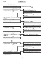
YES
NO
YES
NO
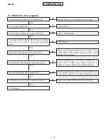
3.0 V
±
0.1 V output at IC002 7 pin?
IC005 Defective.
YES
NO
-10.2 V
±
0.6 V output at TP016, 15.3 V
±
0.9 V at TP015,
and 5.1 V
±
0.1 V at TP014, respectively?
Charge pump regulator IC (IC002) defective.
YES
NO
Are amplitude waveforms of IC003 terminals normal as
shown below?
18 pin: 2.7 Vpp (offset value 0V)
17 pin: 1.12 Vpp (offset value -0.06 V)
16 pin: 0.24 Vpp (offset value -0.07 V)
15 pin: 0.78 Vpp (offset value -0.10 V)
14 pin: 2.86 Vpp (offset value -0.14 V)
Grayscale generator IC (IC003) defective.
YES
NO
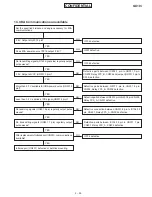
Does output of TP017 to TP027 have pulse waveforms?
IC005 Defective.
Display defective. Or defective mounting of connector
CN002.
NO
YES
Does the display function after replacement?
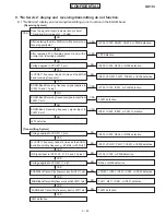
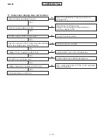
10. Main-screen display does not function.
Main-screen display defective.
YES
NO
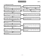
More than 3.2 V applied to TP219?
Refer to Troubleshooting, “Power does not turn on.”
(see page 2-42)
YES
NO
More than 2.8 V
±
0.1 V applied to TP209?
Refer to Troubleshooting, “Power does not turn on.”
(see page 2-42)
YES
NO
More than 2.5 V
±
0.1 V applied to TP009?
Regulator IC004 defective.
YES
NO
13 MHz output at Clock TP011?
0.1V output at both ends of the liquid crystall reset (Jumper
(IC005 40 pin to Q206 2 pin))?
Refer to Troubleshooting, “Power does not turn on.”
(see page 2-42)
IC004 Defective.
Содержание GX10i
Страница 36: ...2 32 GX10i CONFIDENTIAL Point Figure 66 Contact points Push Figure 67 Turning power on ...
Страница 84: ...GX10i CONFIDENTIAL MEMO 4 5 ...
Страница 120: ...5 36 GX10i CONFIDENTIAL MEMO ...


