20
AK - 45
CHASSIS
external components while offering a high flexibility and reliability. The device also features a very high
efficiency stand–by management consisting of an effective Pulsed Mode operation. This technique
enables the reduction of the stand–by power consumption to approximately 1W while delivering
300mW in a 150W SMPS.
• Integrated Start–Up Current Source
• Lossless Off–Line Start–Up
• Direct Off–Line Operation
• Fast Start–Up
13.11.2.General Features
• Flexibility
• Duty Cycle Control
• Under voltage Lockout with Hysteresis
• On Chip Oscillator Switching Frequency 40, or 75kHz
• Secondary Control with Few External Components
Protections
• Maximum Duty Cycle Limitation
• Cycle by Cycle Current Limitation
• Demagnetization (Zero Current Detection) Protection
• “Over V
CC
Protection” Against Open Loop
• Programmable Low Inertia Over Voltage Protection Against Open Loop
• Internal Thermal Protection
GreenLine
TM
Controller
• Pulsed Mode Techniques for a Very High Efficiency Low Power Mode
• Lossless Start-up
• Low dV/dT for Low EMI Radiations
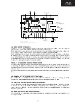
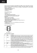
13.11.3.Pin Connections
1
8
7
6
5
2
3
4
(Top View)
Demag
I
sense
Control Input
V
i
GND
V
CC
Driver
44608Pxxx
AW
L
YYWW
AWL
= Manufacturing Code
YYWW = Date Code
(Top View)
13.11.4.Pin Function description
Pin
Name
Description
1
Demag
The Demag pin offers 3 different functions: Zero voltage crossing detection (50mV), 24mA current
detection and 120mA current detection. The 24mA level is used to detect the secondary
reconfiguration status and the 120mA level to detect an Over Voltage status called Quick OVP.
2
ISENSE
The Current Sense pin senses the voltage developed on the series resistor inserted in the source
of the power MOSFET. When I sense reaches 1V, the Driver output (pin 5) is disabled. This is
known as the Over Current Protection function. A 200mA current source is flowing out of the pin 3
during the start–up phase and during the switching phase in case of the Pulsed Mode of operation.
A resistor can be inserted between the sense resistor and the pin 3; thus a programmable peak
current detection can be performed during the SMPS stand–by mode.
3
Control Input
A feedback current from the secondary side of the SMPS via the opto–coupler is injected into this
pin. A resistor can be connected between this pin and GND to allow the programming of the Burst
duty cycle during the Stand–by mode.
4
Ground
This pin is the ground of the primary side of the SMPS.
5
Driver
The current and slew rate capability of this pin are suited to drive Power MOSFETs.
6
VCC
This pin is the positive supply of the IC. The driver output gets disabled when the voltage becomes
higher than 15V and the operating range is between 6.6V and 13V. An intermediate voltage level
of 10V creates a disabling condition called Latched Off phase.
7
This pin is to provide isolation between the Vi pin 8 and the VCC pin 6.
8
Vi
This pin can be directly connected to a 500V voltage source for start–up function of the IC. During
the Start–up phase a 9 mA current source is internally delivered to the VCC pin 6 allowing a rapid
charge of the VCC capacitor. As soon as the IC starts–up, this current source is disabled.
Содержание C-2890EES
Страница 7: ...7 C 2890EES CHASSIS LAYOUT Mother Unit CRT Unit Control Panel Unit ...
Страница 69: ...53 AK 45 CHASSIS 14 6 GEOMETRY ADJUSTMENT 4 3 FORMATS 4 3 MODE 16 9 MODE ...
Страница 70: ...54 AK 45 CHASSIS 16 9 FORMATS AUTO MODE ...
Страница 71: ...55 AK 45 CHASSIS REGULAR MODE ...
Страница 72: ...56 AK 45 CHASSIS ZOOM 14 9 MODE ...
Страница 73: ...57 AK 45 CHASSIS ZOOM 16 9 MODE ...
Страница 74: ...58 AK 45 CHASSIS SUBTITLE ZOOM MODE ...
Страница 75: ...59 AK 45 CHASSIS FULL MODE ...
Страница 76: ...60 AK 45 CHASSIS PANORAMIC MODE ...
Страница 79: ...63 AK 45 CHASSIS 8 9 10 11 12 13 14 I H G F E D C B A Page 62 16 1 Schematic Diagram of Video IF Circuit ...
Страница 80: ...64 AK 45 CHASSIS 16 2 Schematic Diagram of µ Controller Circuit 1 I H G F E D C B A 2 3 4 5 6 7 ...
Страница 82: ...66 AK 45 CHASSIS 1 I H G F E D C B A 2 3 4 5 6 7 Page 67 16 5 Schematic Diagram of SMPS Circuit ...
Страница 83: ...67 AK 45 CHASSIS 8 9 10 11 12 13 14 I H G F E D C B A Page 66 16 5 Schematic Diagram of SMPS Circuit ...
Страница 84: ...68 AK 45 CHASSIS 1 I H G F E D C B A 2 3 4 5 6 7 Page 69 16 6 Schematic Diagram of Sound Circuit ...
Страница 85: ...69 AK 45 CHASSIS 8 9 10 11 12 13 14 I H G F E D C B A Page 68 16 6 Schematic Diagram of Sound Circuit ...
Страница 86: ...70 AK 45 CHASSIS 1 I H G F E D C B A 2 3 4 5 6 7 16 7 Schematic Diagram of CRT Socket Circuit ...
Страница 87: ...71 AK 45 CHASSIS 8 9 10 11 12 13 14 I H G F E D C B A 16 8 Schematic Diagrams of Control Panel Unit ...
Страница 88: ...72 AK 45 CHASSIS 1 I H G F E D C B A 2 3 4 5 6 7 16 9 Schematic Diagram of Remote Control Circuit ...
Страница 91: ...75 AK 45 CHASSIS Notes ...


