14
AK - 45
CHASSIS
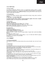
13.4.2.Features
Video Decoding and Processing
– four CVBS, one S-VHS input, one YC
R
C
B
component input
– integrated high-quality A/D converters and associated clamp and AGC circuits
– adaptive 2H comb filter Y/C separator
– multistandard colour decoder PAL/NTSC/SECAM including all substandards
– multistandard sync decoder
– automatic standard recognition
– black-line detector
– linear horizontal scaling (0.25...4), as well as non-linear horizontal scaling “Panoramavision”
– black-level expander
– dynamic peaking
– soft limiter (gamma correction)
– colour transient improvement
RGB Processing and Deflection
– programmable RGB matrix
– two analog RGB / Fastblank inputs
– half-contrast switch
– picture frame generator
– scan velocity modulation output
– high-performance H/V deflection
– separate ADC for tube measurements
– EHT compensation
– angle and bow correction
– one 20.25 MHz crystal, few external components
–I
2
C-Bus Interface
– 64-pin PSDIP package
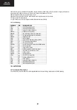
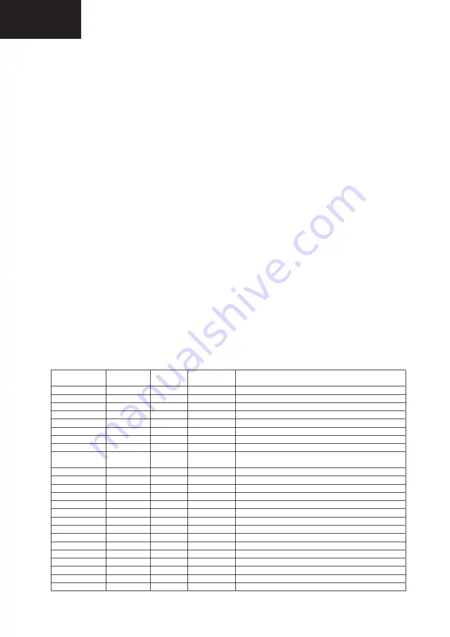
13.4.3.Pin Connections and short descriptions
NC = not connected
LV = if not used, leave vacant
X = obligatory; connect as described in circuit diagram
IN = Input
OUT
=
Output
SUPPLY
=
Supply
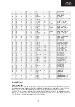
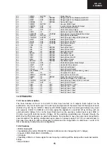
Pin
Pin no
PSDIP 64-pin
Pin name
Type
Connection
(if not used)
Short description
1 TEST
IN
GNDD
Test
Input
2 RESQ
IN
X
Reset
Input
3 SCL
IN/OUT
X
I
2
C Bus Clock
4 SDA
IN/OUT
X
I
2
C Bus Data
5 GNDD
SUPPLY
X
Digital
Ground
6
HCS
IN
LV
Half Contrast Switch Input
7
FSY
OUT
LV
Front Sync Output
8
CSY
OUT
LV
Composite Sync Output
9
VS
OUT
LV
Vertical Sync Output
(=VS Bit of MSY for TPU)
10
INTLC
OUT
LV
Interface Control Output
11
VPROT
IN
GNDAB
Vertical Protection Input
12 SAFETY
IN
GNDAB
Safety
Input
13
HFLB
IN
HOUT
Horizontal Flyback Input
14 GNDD
SUPPLY
X
Digital
Ground
15 VSUPD
SUPPLY
X
Digital
Supply
Voltage
(3.3V)
16 GNDD
SUPPLY
X
Digital
Ground
17
VSUPD
SUPPLY
LV
Digital Supply Voltage (3.3V)
18
P0
IN/OUT
LV
Port 1, Bit 0
19
P1
IN/OUT
LV
Port 1, Bit 1
20
P2
IN/OUT
GNDD
Port 1, Bit 2
21
P3
IN/OUT
GNDD
Port 1, Bit 3
22
P4
IN/OUT
GNDD
Port 1, Bit 4
23
P5
IN/OUT
GNDD
Port 1, Bit 5
24
P6
IN/OUT
GNDD
Port 1, Bit 6
Содержание C-2890EES
Страница 7: ...7 C 2890EES CHASSIS LAYOUT Mother Unit CRT Unit Control Panel Unit ...
Страница 69: ...53 AK 45 CHASSIS 14 6 GEOMETRY ADJUSTMENT 4 3 FORMATS 4 3 MODE 16 9 MODE ...
Страница 70: ...54 AK 45 CHASSIS 16 9 FORMATS AUTO MODE ...
Страница 71: ...55 AK 45 CHASSIS REGULAR MODE ...
Страница 72: ...56 AK 45 CHASSIS ZOOM 14 9 MODE ...
Страница 73: ...57 AK 45 CHASSIS ZOOM 16 9 MODE ...
Страница 74: ...58 AK 45 CHASSIS SUBTITLE ZOOM MODE ...
Страница 75: ...59 AK 45 CHASSIS FULL MODE ...
Страница 76: ...60 AK 45 CHASSIS PANORAMIC MODE ...
Страница 79: ...63 AK 45 CHASSIS 8 9 10 11 12 13 14 I H G F E D C B A Page 62 16 1 Schematic Diagram of Video IF Circuit ...
Страница 80: ...64 AK 45 CHASSIS 16 2 Schematic Diagram of µ Controller Circuit 1 I H G F E D C B A 2 3 4 5 6 7 ...
Страница 82: ...66 AK 45 CHASSIS 1 I H G F E D C B A 2 3 4 5 6 7 Page 67 16 5 Schematic Diagram of SMPS Circuit ...
Страница 83: ...67 AK 45 CHASSIS 8 9 10 11 12 13 14 I H G F E D C B A Page 66 16 5 Schematic Diagram of SMPS Circuit ...
Страница 84: ...68 AK 45 CHASSIS 1 I H G F E D C B A 2 3 4 5 6 7 Page 69 16 6 Schematic Diagram of Sound Circuit ...
Страница 85: ...69 AK 45 CHASSIS 8 9 10 11 12 13 14 I H G F E D C B A Page 68 16 6 Schematic Diagram of Sound Circuit ...
Страница 86: ...70 AK 45 CHASSIS 1 I H G F E D C B A 2 3 4 5 6 7 16 7 Schematic Diagram of CRT Socket Circuit ...
Страница 87: ...71 AK 45 CHASSIS 8 9 10 11 12 13 14 I H G F E D C B A 16 8 Schematic Diagrams of Control Panel Unit ...
Страница 88: ...72 AK 45 CHASSIS 1 I H G F E D C B A 2 3 4 5 6 7 16 9 Schematic Diagram of Remote Control Circuit ...
Страница 91: ...75 AK 45 CHASSIS Notes ...

