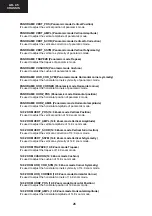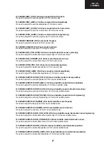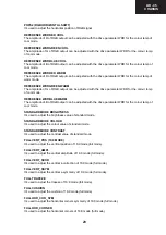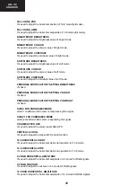
15
AK - 45
CHASSIS
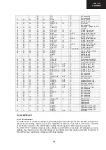
25 GNDD
SUPPLY
X
Digital
Ground
26
RSW2
OUT
GNDAB
Range Switch 2 for Measurement ADC
27
RSW1
OUT
GNDAB
Range Switch 1 for Measurement ADC
28
SENSE
IN
GNDAB
Sense ADC Input
29
GNDM
SUPPLY
X
Ground, MADC Input
30
VERTQ
OUT
LV
Inverted Vertical Sawtooth Output
31
VERT
OUT
LV
Vertical Sawtooth Output
32
E/w
OUT
LV
Vertical Parabola Output
33
XREF
IN
X
Reference Input for RGB DACs
34
SVMOUT
OUT
VSUPAB
Analog Scan Velocity Modulation Output
35
GNDAB
SUPPLY
X
Analog Ground Backend
36
VSUPAB
SUPPLY
X
Analog Supply Voltage (5.0V) Backend
37
ROUT
OUT
VSUPAB
Analog Red Output
38
GOUT
OUT
VSUPAB
Analog Green Output
39
BOUT
OUT
VSUPAB
Analog Blue Output
40 VRD
IN
X
DAC
Reference
41
RIN
IN
GNDAB
Analog Red Input
42
GIN
IN
GNDAB
Analog Green Input
43
BIN
IN
GNDAB
Analog Blue Input
44
FBLIN
IN
GNDAB
Fast Blank Input
45
RIN2
IN
GNDAB
Analog Red Input2
46
GIN2
IN
GNDAB
Analog Green Input2
47
BIN2
IN
GNDAB
Analog Blue Input2
48
FBLIN2
IN
GNDAB
Fast Blank Input2
49
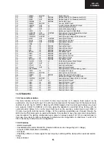
CLK20
OUT
LV
20.25 MHz System Clock Output
50
HOUT
OUT
X
Horizontal Drive Output
51
XTAL 1
IN
X
Analog Crystal Input
52
XTAL 2
OUT
X
Analog Crystal Output
53
CIN 2/CRIN
LV
Analog Chroma 2/Component C
R
Input
54 CBIN
IN
LV
Component
C
B
Input
55
GNDAF
SUPPLY
X
Analog Ground Front-end
56
SGND
IN
GNDAF
Signal Ground for Analog Input
57
VRT
IN
X
Reference Voltage Top, Video ADC
58
VSUPAF
SUPPLY
X
Analog Supply Voltage (5.0V) Front-end
59 VOUT
OUT
LV
Analog
Video
Output
60
CIN1
IN
VRT
Analog Chroma 1 Input
61
VIN1
IN
VRT
Analog Video 1 Input
62
VIN2
IN
VRT
Analog Video 2 Input
63
VIN3
IN
VRT
Analog Video 3 Input
64
VIN4
IN
VRT
Analog Video 4 Input
13.5.TEA6415C
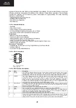
13.5.1.General Description
The main function of the IC is to switch 8 video input sources on 6 outputs. Each output can be
switched on only one of each input. On each input an alignment of the lowest level of the signal is made
(bottom of synch. top for CVBS or black level for RGB signals). Each nominal gain between any input
and output is 6.5dB. For D2MAC or Chroma signal the alignment is switched off by forcing, with an
external resistor bridge, 5 V
DC
on the input. Each input can be used as a normal input or as a MAC or
Chroma input (with external resistor bridge). All the switching possibilities are changed through the
BUS. Driving 75
load needs an external transistor. It is possible to have the same input connected to
several outputs. The starting configuration upon power on (power supply: 0 to 10V) is undetermined. In
this case, 6 words of 16 bits are necessary to determine one configuration. In other case, 1 word of 16
bits is necessary to determine one configuration.
13.5.2.Features
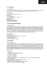
• 20MHz Bandwidth
• Cascadable with another TEA6415C (Internal address can be changed by pin 7 voltage)
• 8 Inputs (CVBS, RGB, MAC, CHROMA,...)
• 6 Outputs
• Possibility of MAC or chroma signal for each input by switching-off the clamp with an external resistor
bridge
• Bus controlled
Содержание C-2890EES
Страница 7: ...7 C 2890EES CHASSIS LAYOUT Mother Unit CRT Unit Control Panel Unit ...
Страница 69: ...53 AK 45 CHASSIS 14 6 GEOMETRY ADJUSTMENT 4 3 FORMATS 4 3 MODE 16 9 MODE ...
Страница 70: ...54 AK 45 CHASSIS 16 9 FORMATS AUTO MODE ...
Страница 71: ...55 AK 45 CHASSIS REGULAR MODE ...
Страница 72: ...56 AK 45 CHASSIS ZOOM 14 9 MODE ...
Страница 73: ...57 AK 45 CHASSIS ZOOM 16 9 MODE ...
Страница 74: ...58 AK 45 CHASSIS SUBTITLE ZOOM MODE ...
Страница 75: ...59 AK 45 CHASSIS FULL MODE ...
Страница 76: ...60 AK 45 CHASSIS PANORAMIC MODE ...
Страница 79: ...63 AK 45 CHASSIS 8 9 10 11 12 13 14 I H G F E D C B A Page 62 16 1 Schematic Diagram of Video IF Circuit ...
Страница 80: ...64 AK 45 CHASSIS 16 2 Schematic Diagram of µ Controller Circuit 1 I H G F E D C B A 2 3 4 5 6 7 ...
Страница 82: ...66 AK 45 CHASSIS 1 I H G F E D C B A 2 3 4 5 6 7 Page 67 16 5 Schematic Diagram of SMPS Circuit ...
Страница 83: ...67 AK 45 CHASSIS 8 9 10 11 12 13 14 I H G F E D C B A Page 66 16 5 Schematic Diagram of SMPS Circuit ...
Страница 84: ...68 AK 45 CHASSIS 1 I H G F E D C B A 2 3 4 5 6 7 Page 69 16 6 Schematic Diagram of Sound Circuit ...
Страница 85: ...69 AK 45 CHASSIS 8 9 10 11 12 13 14 I H G F E D C B A Page 68 16 6 Schematic Diagram of Sound Circuit ...
Страница 86: ...70 AK 45 CHASSIS 1 I H G F E D C B A 2 3 4 5 6 7 16 7 Schematic Diagram of CRT Socket Circuit ...
Страница 87: ...71 AK 45 CHASSIS 8 9 10 11 12 13 14 I H G F E D C B A 16 8 Schematic Diagrams of Control Panel Unit ...
Страница 88: ...72 AK 45 CHASSIS 1 I H G F E D C B A 2 3 4 5 6 7 16 9 Schematic Diagram of Remote Control Circuit ...
Страница 91: ...75 AK 45 CHASSIS Notes ...

